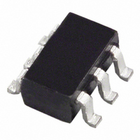
AD7476ARTZ-500RL7 Analog Devices Inc, AD7476ARTZ-500RL7 Datasheet - Page 12

AD7476ARTZ-500RL7
Manufacturer Part Number
AD7476ARTZ-500RL7
Description
IC ADC 12BIT 1MSPS SOT-23-6
Manufacturer
Analog Devices Inc
Datasheet
1.AD7476ARTZ-500RL7.pdf
(20 pages)
Specifications of AD7476ARTZ-500RL7
Data Interface
DSP, MICROWIRE™, QSPI™, Serial, SPI™
Design Resources
Output Channel Monitoring Using AD5380 (CN0008) AD5382 Channel Monitor Function (CN0012) AD5381 Channel Monitor Function (CN0013) AD5383 Channel Monitor Function (CN0015) AD5390/91/92 Channel Monitor Function (CN0030) Power off protected data acquisition signal chain using ADG4612 , AD711, and AD7476 (CN0165)
Number Of Bits
12
Sampling Rate (per Second)
1M
Number Of Converters
1
Power Dissipation (max)
17.5mW
Voltage Supply Source
Single Supply
Operating Temperature
-40°C ~ 85°C
Mounting Type
Surface Mount
Package / Case
SOT-23-6
Resolution (bits)
12bit
Sampling Rate
1MSPS
Input Channel Type
Single Ended
Supply Voltage Range - Analog
2.7V To 5.25V
Supply Current
3.5mA
Lead Free Status / RoHS Status
Lead free / RoHS Compliant
For Use With
EVAL-AD7476ACBZ - BOARD EVALUATION FOR AD7476AAD7476-DBRD - BOARD EVAL FOR AD7476AD7476A-DBRD - BOARD EVAL FOR AD7476A
Lead Free Status / RoHS Status
Lead free / RoHS Compliant, Lead free / RoHS Compliant
Other names
AD7476ARTZ-500RL7TR
Available stocks
Company
Part Number
Manufacturer
Quantity
Price
Company:
Part Number:
AD7476ARTZ-500RL7
Manufacturer:
ADI
Quantity:
2
AD7476/AD7477/AD7478
Digital Inputs
The digital inputs applied to the AD7476/AD7477/AD7478 are
not limited by the maximum ratings that limit the analog inputs.
Instead, the digital inputs applied can go to 7 V and are not
Figure 10. THD vs. Analog Input Frequency, f
Figure 9. THD vs. Analog Input Frequency, f
–50
–55
–60
–65
–70
–75
–80
–85
–90
–72
–74
–76
–78
–80
–82
–84
10k
10k
INPUT FREQUENCY – Hz
INPUT FREQUENCY – Hz
SDATA
SDATA
SCLK
SCLK
100k
100k
CS
CS
V
DD
= 5.25V
V
V
DD
V
DD
DD
Figure 12. Entering Power-Down Mode
= 2.7V
V
V
V
= 2.35V
DD
1
DD
DD
1
V
= 3.6V
V
Figure 11. Normal Mode Operation
V
DD
DD
DD
= 3.6V
= 4.75V
= 5.25V
S
2
S
= 4.75V
= 2.35V
= 2.7V
= 993 kSPS
= 605 kSPS
4 LEADING ZEROS + CONVERSION RESULT
1M
1M
–12–
restricted by the V
example, if the AD7476/AD7477/AD7478 were operated with a
V
inputs. However, it is important to note that the data output on
SDATA will still have 3 V logic levels when V
advantage of SCLK and CS not being restricted by the V
0.3 V limit is the fact that power supply sequencing issues are
avoided. If CS or SCLK is applied before V
latch-up as there would be on the analog inputs if a signal greater
than 0.3 V was applied prior to V
MODES OF OPERATION
The mode of operation of the AD7476/AD7477/AD7478 is
selected by controlling the (logic) state of the CS signal during a
conversion. There are two possible modes of operation, Normal
mode and Power-Down mode. The point at which CS is pulled
high after the conversion has been initiated will determine whether
or not the AD7476/AD7477/AD7478 will enter Power-Down
mode. Similarly, if already in power-down, CS can control
whether the device will return to normal operation or remain in
power-down. These modes of operation are designed to provide
flexible power management options. These options can be chosen
to optimize the power dissipation/throughput rate ratio for different
application requirements.
Normal Mode
This mode is intended for fastest throughput rate performance,
as the user does not have to worry about any power-up times
with the AD7476/AD7477/AD7478 remaining fully powered all
the time. Figure 11 shows the general diagram of the operation
of the AD7476/AD7477/AD7478 in this mode.
The conversion is initiated on the falling edge of CS as described
in the Serial Interface section. To ensure the part remains fully
powered up at all times, CS must remain low until at least 10
SCLK falling edges have elapsed after the falling edge of CS. If
CS is brought high any time after the tenth SCLK falling edge,
but before the sixteenth SCLK falling edge, the part will remain
powered up but the conversion will be terminated and SDATA
will go back into three-state. Sixteen serial clock cycles are
required to complete the conversion and access the complete
DD
of 3 V, then 5 V logic levels could be used on the digital
10
THREE-STATE
10
DD
+ 0.3 V limit as on the analog inputs. For
16
16
DD
.
DD
DD
, there is no risk of
= 3 V. Another
REV. D
DD
+


