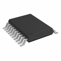
AD7328BRUZ Analog Devices Inc, AD7328BRUZ Datasheet - Page 16

AD7328BRUZ
Manufacturer Part Number
AD7328BRUZ
Description
IC ADC 12BIT+ SAR 8CHAN 20TSSOP
Manufacturer
Analog Devices Inc
Specifications of AD7328BRUZ
Data Interface
DSP, MICROWIRE™, QSPI™, Serial, SPI™
Design Resources
Using AD7328 in Appls with Single-Ended Industrial-Level Signals (CN0047)
Number Of Bits
12
Sampling Rate (per Second)
1M
Number Of Converters
1
Power Dissipation (max)
30mW
Voltage Supply Source
Dual ±
Operating Temperature
-40°C ~ 85°C
Mounting Type
Surface Mount
Package / Case
20-TSSOP (0.173", 4.40mm Width)
Resolution (bits)
13bit
Sampling Rate
1MSPS
Input Channel Type
Pseudo Differential, Single Ended
Supply Current
900µA
Digital Ic Case Style
TSSOP
No. Of Pins
20
Lead Free Status / RoHS Status
Lead free / RoHS Compliant
For Use With
EVAL-AD7328CBZ - BOARD EVALUATION FOR AD7328
Lead Free Status / Rohs Status
RoHS Compliant part
Electrostatic Device
Available stocks
Company
Part Number
Manufacturer
Quantity
Price
Part Number:
AD7328BRUZ
Manufacturer:
ADI/亚德诺
Quantity:
20 000
Company:
Part Number:
AD7328BRUZ-REEL7
Manufacturer:
ALLEGRO
Quantity:
1 200
AD7328
Figure 25 shows the differential configuration during the ac-
quisition phase. For the conversion phase, SW3 opens and SW1
and SW2 move to Position B (see Figure 26). The output
impedances of the source driving the V
match; otherwise, the two inputs have different settling times,
resulting in errors.
Output Coding
The AD7328 default output coding is set to twos complement.
The output coding is controlled by the coding bit in the control
register. To change the output coding to straight binary coding,
the coding bit in the control register must be set. When operating
in sequence mode, the output coding for each channel in the
sequence is the value written to the coding bit during the last
write to the control register.
Transfer Functions
The designed code transitions occur at successive integer
LSB values (that is, 1 LSB, 2 LSB, and so on). The LSB size
is dependent on the analog input range selected.
Table 7. LSB Sizes for Each Analog Input Range
Input Range
±10 V
±5 V
±2.5 V
0 V to +10 V
Figure 25. ADC Differential Configuration During Acquisition Phase
Figure 26. ADC Differential Configuration During Conversion Phase
V
V
V
V
V
IN
IN
IN
IN
IN
+
+
0
–
–
Figure 24. ADC Conversion Phase (Single-Ended)
AGND
B
B
B
V
B
B
V
A
A
A
A
A
REF
REF
SW1
SW2
SW1
SW2
SW1
Full-Scale Range/8192 Codes
20 V
10 V
5 V
10 V
C
C
C
C
C
S
S
S
S
S
SW2
SW3
SW3
COMPARATOR
COMPARATOR
COMPARATOR
IN
+ and V
CAPACITIVE
CAPACITIVE
CAPACITIVE
CAPACITIVE
CAPACITIVE
CONTROL
CONTROL
CONTROL
LOGIC
LOGIC
LOGIC
DAC
DAC
DAC
DAC
DAC
IN
− pins must
LSB Size
2.441 mV
1.22 mV
0.61 mV
1.22 mV
Rev. A | Page 16 of 36
The ideal transfer characteristic for the AD7328 when twos
complement coding is selected is shown in Figure 27. The ideal
transfer characteristic for the AD7328 when straight binary coding
is selected is shown in Figure 28.
ANALOG INPUT STRUCTURE
The analog inputs of the AD7328 can be configured as single-
ended, true differential, or pseudo differential via the control
register mode bits (see Table 10). The AD7328 can accept true
bipolar input signals. On power-up, the analog inputs operate as
eight single-ended analog input channels. If true differential or
pseudo differential is required, a write to the control register is
necessary after power-up to change this configuration.
Figure 29 shows the equivalent analog input circuit of the
AD7328 in single-ended mode. Figure 30 shows the equivalent
analog input structure in differential mode. The two diodes
provide ESD protection for the analog inputs.
Figure 27. Twos Complement Transfer Characteristic (Bipolar Ranges)
Figure 28. Straight Binary Transfer Characteristic (Bipolar Ranges)
000...001
000...000
100...010
100...001
100...000
000...010
000...001
000...000
011...110
111...000
Figure 29. Equivalent Analog Input Circuit (Single-Ended)
011...111
111...111
111...111
111...110
011...111
–FSR/2 + 1LSB
AGND + 1LSB
V
IN
0
–FSR/2 + 1LSB
AGND + 1LSB
AGND – 1LSB
C1
ANALOG INPUT
ANALOG INPUT
V
V
DD
SS
D
D
+FSR/2 – 1LSB BIPOLAR RANGES
+FSR – 1LSB
+FSR/2 – 1LSB BIPOLAR RANGES
+FSR – 1LSB
R1
UNIPOLAR RANGE
UNIPOLAR RANGE
C2


