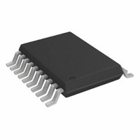
AD7328BRUZ Analog Devices Inc, AD7328BRUZ Datasheet - Page 5

AD7328BRUZ
Manufacturer Part Number
AD7328BRUZ
Description
IC ADC 12BIT+ SAR 8CHAN 20TSSOP
Manufacturer
Analog Devices Inc
Specifications of AD7328BRUZ
Data Interface
DSP, MICROWIRE™, QSPI™, Serial, SPI™
Design Resources
Using AD7328 in Appls with Single-Ended Industrial-Level Signals (CN0047)
Number Of Bits
12
Sampling Rate (per Second)
1M
Number Of Converters
1
Power Dissipation (max)
30mW
Voltage Supply Source
Dual ±
Operating Temperature
-40°C ~ 85°C
Mounting Type
Surface Mount
Package / Case
20-TSSOP (0.173", 4.40mm Width)
Resolution (bits)
13bit
Sampling Rate
1MSPS
Input Channel Type
Pseudo Differential, Single Ended
Supply Current
900µA
Digital Ic Case Style
TSSOP
No. Of Pins
20
Lead Free Status / RoHS Status
Lead free / RoHS Compliant
For Use With
EVAL-AD7328CBZ - BOARD EVALUATION FOR AD7328
Lead Free Status / Rohs Status
RoHS Compliant part
Electrostatic Device
Available stocks
Company
Part Number
Manufacturer
Quantity
Price
Part Number:
AD7328BRUZ
Manufacturer:
ADI/亚德诺
Quantity:
20 000
Company:
Part Number:
AD7328BRUZ-REEL7
Manufacturer:
ALLEGRO
Quantity:
1 200
Parameter
LOGIC INPUTS
LOGIC OUTPUTS
CONVERSION RATE
POWER REQUIREMENTS
POWER DISSIPATION
1
2
3
4
5
6
Temperature range is −40°C to +85°C.
See the Terminology section.
Sample tested during initial release to ensure compliance.
For dc accuracy specifications, the LSB size for differential mode is FSR/8192. For single-ended mode/pseudo differential mode, the LSB size is FSR/4096, unless otherwise noted.
Unipolar 0 V to 10 V range with straight binary output coding.
Bipolar range with twos complement output coding.
Input High Voltage, V
Input Low Voltage, V
Input Current, I
Input Capacitance, C
Output High Voltage, V
Output Low Voltage, V
Floating-State Leakage Current
Floating-State Output
Output Coding
Conversion Time
Track-and-Hold Acquisition
Throughput Rate
V
V
V
V
Normal Mode (Static)
Normal Mode (Operational)
Autostandby Mode (Dynamic)
Autoshutdown Mode (Static)
Full Shutdown Mode
Normal Mode
Full Shutdown Mode
Capacitance
DD
SS
CC
DRIVE
Time
I
I
I
I
I
I
I
I
I
I
I
I
DD
SS
CC
DD
SS
CC
DD
SS
CC
DD
SS
CC
and I
and I
and I
and I
2, 3
1
DRIVE
DRIVE
DRIVE
DRIVE
3
IN
INL
IN
INH
3
OL
OH
Min
2.4
V
0.2
12
−12
2.7
2.7
DRIVE
−
Straight natural binary
Twos complement
B Version
Typ
10
5
0.9
21
Rev. A | Page 5 of 36
Max
0.8
0.4
±1
0.4
±1
800
305
1
770
16.5
−16.5
5.25
5.25
360
410
3.2
200
210
1.3
1
1
1
1
1
1
30
38.25
Unit
V
V
V
μA
pF
V
V
μA
pF
ns
ns
MSPS
kSPS
V
V
V
V
mA
μA
μA
mA
μA
μA
mA
μA
μA
μA
μA
μA
μA
mW
mW
μW
Test Conditions/Comments
V
V
V
I
I
Coding bit set to 1 in control register
Coding bit set to 0 in control register
16 SCLK cycles with SCLK = 20 MHz
Full-scale step input; see the Terminology section
See the Serial Interface section; V
V
Digital inputs = 0 V or V
See Table 6
See Table 6
See Table 6; typical specifications for V
V
f
V
V
V
f
V
V
V
SCLK on or off
V
V
V
SCLK on or off
V
V
V
V
V
V
SOURCE
SINK
SAMPLE
SAMPLE
CC
CC
IN
CC
DD
DD
SS
CC
DD
SS
CC
DD
SS
CC
DD
SS
CC
DD
DD
DD
/V
/V
/V
/V
= 0 V or V
/V
= −16.5 V
= −16.5 V
= −16.5 V
= −16.5 V
= 4.75 V to 5.25 V
= 2.7 to 3.6 V
< 4.75 V
= 16.5 V
= 16.5 V
= 16.5 V
= 16.5 V
= 16.5 V, V
= 12 V, V
= 16.5 V, V
= 200 μA
DRIVE
DRIVE
DRIVE
DRIVE
SS
= 250 kSPS
= 200 μA
= 1 MSPS
= ±16.5 V, V
= 5.25 V
= 5.25 V
= 5.25 V
= 5.25 V
SS
DRIVE
SS
SS
= −12 V, V
= −16.5 V, V
= −16.5 V, V
CC
/V
DRIVE
DRIVE
CC
= 5 V
= 5.25 V
CC
CC
= 5.25 V
= 5.25 V
CC
= 4.75 V to 5.25 V
CC
< 4.75 V
AD7328


