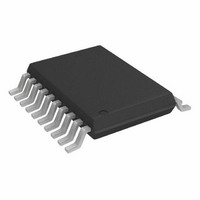
AD7328BRUZ Analog Devices Inc, AD7328BRUZ Datasheet - Page 8

AD7328BRUZ
Manufacturer Part Number
AD7328BRUZ
Description
IC ADC 12BIT+ SAR 8CHAN 20TSSOP
Manufacturer
Analog Devices Inc
Specifications of AD7328BRUZ
Data Interface
DSP, MICROWIRE™, QSPI™, Serial, SPI™
Design Resources
Using AD7328 in Appls with Single-Ended Industrial-Level Signals (CN0047)
Number Of Bits
12
Sampling Rate (per Second)
1M
Number Of Converters
1
Power Dissipation (max)
30mW
Voltage Supply Source
Dual ±
Operating Temperature
-40°C ~ 85°C
Mounting Type
Surface Mount
Package / Case
20-TSSOP (0.173", 4.40mm Width)
Resolution (bits)
13bit
Sampling Rate
1MSPS
Input Channel Type
Pseudo Differential, Single Ended
Supply Current
900µA
Digital Ic Case Style
TSSOP
No. Of Pins
20
Lead Free Status / RoHS Status
Lead free / RoHS Compliant
For Use With
EVAL-AD7328CBZ - BOARD EVALUATION FOR AD7328
Lead Free Status / Rohs Status
RoHS Compliant part
Electrostatic Device
Available stocks
Company
Part Number
Manufacturer
Quantity
Price
Part Number:
AD7328BRUZ
Manufacturer:
ADI/亚德诺
Quantity:
20 000
Company:
Part Number:
AD7328BRUZ-REEL7
Manufacturer:
ALLEGRO
Quantity:
1 200
AD7328
PIN CONFIGURATION AND FUNCTION DESCRIPTIONS
Table 5. Pin Function Descriptions
Pin No.
1
2
3, 19
4
5
6
7, 8, 14, 13, 9, 10,
12, 11
15
16
17
18
20
Mnemonic
CS
DIN
DGND
AGND
REFIN/OUT
V
V
V
V
V
DOUT
SCLK
SS
IN
DD
CC
DRIVE
0 to V
IN
7
Description
Chip Select. Active low logic input. This input provides the dual function of initiating conversions on
the AD7328 and frames the serial data transfer.
Data In. Data to be written to the on-chip registers is provided on this input and is clocked into the
register on the falling edge of SCLK (see the Registers section).
Digital Ground. Ground reference point for all digital circuitry on the AD7328. The DGND and AGND
voltages should ideally be at the same potential and must not be more than 0.3 V apart, even on a
transient basis.
Analog Ground. Ground reference point for all analog circuitry on the AD7328. All analog input signals
and any external reference signal should be referred to this AGND voltage. The AGND and DGND voltages
should ideally be at the same potential and must not be more than 0.3 V apart, even on a transient basis.
Reference Input/Reference Output. The on-chip reference is available on this pin for use external to the
AD7328. The nominal internal reference voltage is 2.5 V, which appears at the pin. A 680 nF capacitor
should be placed on the reference pin. Alternatively, the internal reference can be disabled and an
external reference applied to this input. On power-up, the external reference mode is the default
condition (see the Reference section).
Negative Power Supply Voltage. This is the negative supply voltage for the analog input section.
Analog Input 0 to Analog Input 7. The analog inputs are multiplexed into the on-chip track-and-hold.
The analog input channel for conversion is selected by programming the Channel Address Bit ADD2
through Bit ADD0 in the control register. The inputs can be configured as eight single-ended inputs,
four true differential input pairs, four pseudo differential inputs, or seven pseudo differential inputs.
The configuration of the analog inputs is selected by programming the mode bits, Bit Mode 1 and
Bit Mode 0, in the control register. The input range on each input channel is controlled by program-
ming the range registers. Input ranges of ±10 V, ±5 V, ±2.5 V, and 0 V to +10 V can be selected on each
analog input channel when a +2.5 V reference voltage is used (see the Reference section).
Positive Power Supply Voltage. This is the positive supply voltage for the analog input section.
Analog Supply Voltage, 2.7 V to 5.25 V. This is the supply voltage for the ADC core on the AD7328.
This supply should be decoupled to AGND. Specifications apply from V
Logic Power Supply Input. The voltage supplied at this pin determines at what voltage the interface
operates. This pin should be decoupled to DGND. The voltage at this pin may be different to that at V
but it should not exceed V
Serial Data Output. The conversion output data is supplied to this pin as a serial data stream. The bits
are clocked out on the falling edge of the SCLK input, and 16 SCLKs are required to access the data. The
data stream consists of three channel identification bits, the sign bit, and 12 bits of conversion data.
The data is provided MSB first (see the Serial Interface section).
Serial Clock, Logic Input. A serial clock input provides the SCLK used for accessing the data from the
AD7328. This clock is also used as the clock source for the conversion process.
REFIN/OUT
Figure 3. TSSOP Pin Configuration
DGND
AGND
V
V
V
V
DIN
V
CS
IN
IN
IN
IN
SS
0
1
4
5
Rev. A | Page 8 of 36
10
1
2
3
4
5
6
7
8
9
CC
by more than 0.3 V.
(Not to Scale)
TOP VIEW
AD7328
15
14
13
12
11
20
19
18
17
16
SCLK
DGND
DOUT
V
V
V
V
V
V
V
DRIVE
CC
DD
IN
IN
IN
IN
2
3
6
7
CC
= 4.75 V to 5.25 V.
CC
,


