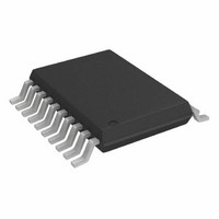
AD7328BRUZ Analog Devices Inc, AD7328BRUZ Datasheet - Page 18

AD7328BRUZ
Manufacturer Part Number
AD7328BRUZ
Description
IC ADC 12BIT+ SAR 8CHAN 20TSSOP
Manufacturer
Analog Devices Inc
Specifications of AD7328BRUZ
Data Interface
DSP, MICROWIRE™, QSPI™, Serial, SPI™
Design Resources
Using AD7328 in Appls with Single-Ended Industrial-Level Signals (CN0047)
Number Of Bits
12
Sampling Rate (per Second)
1M
Number Of Converters
1
Power Dissipation (max)
30mW
Voltage Supply Source
Dual ±
Operating Temperature
-40°C ~ 85°C
Mounting Type
Surface Mount
Package / Case
20-TSSOP (0.173", 4.40mm Width)
Resolution (bits)
13bit
Sampling Rate
1MSPS
Input Channel Type
Pseudo Differential, Single Ended
Supply Current
900µA
Digital Ic Case Style
TSSOP
No. Of Pins
20
Lead Free Status / RoHS Status
Lead free / RoHS Compliant
For Use With
EVAL-AD7328CBZ - BOARD EVALUATION FOR AD7328
Lead Free Status / Rohs Status
RoHS Compliant part
Electrostatic Device
Available stocks
Company
Part Number
Manufacturer
Quantity
Price
Part Number:
AD7328BRUZ
Manufacturer:
ADI/亚德诺
Quantity:
20 000
Company:
Part Number:
AD7328BRUZ-REEL7
Manufacturer:
ALLEGRO
Quantity:
1 200
AD7328
TYPICAL CONNECTION DIAGRAM
Figure 32 shows a typical connection diagram for the AD7328.
In this configuration, the AGND pin is connected to the analog
ground plane of the system, and the DGND pin is connected to
the digital ground plane of the system. The analog inputs on the
AD7328 can be configured to operate in single-ended, true dif-
ferential, or pseudo differential mode. The AD7328 can operate
with either an internal or external reference. In Figure 32, the
AD7328 is configured to operate with the internal 2.5 V reference.
A 680 nF decoupling capacitor is required when operating with
the internal reference.
The V
V
input structures. The voltage on these pins must be equal to or
greater than the highest analog input range selected on the analog
input channels (see Table 6 for more information). The V
is connected to the supply voltage of the microprocessor. The
voltage applied to the V
serial interface. V
+15V
–15V
ANALOG INPUT
Single-Ended Inputs
The AD7328 has a total of eight analog inputs when operating
in single-ended mode. Each analog input can be independently
programmed to one of the four analog input ranges. In applications
where the signal source is high impedance, it is recommended
to buffer the signal before applying it to the ADC analog inputs.
Figure 33 shows the configuration of the AD7328 in single-
ended mode.
DD
ANALOG INPUTS:
±10V, ±5V, ±2.5V,
0V TO +10V
and V
CC
680nF
pin can be connected to either a 3 V or 5 V supply voltage.
0.1µF
0.1µF
SS
are the dual supplies for the high voltage analog
Figure 32. Typical Connection Diagram
+
+
10µF
10µF
DRIVE
V
V
V
V
V
V
V
V
REFIN/OUT
IN
IN
IN
IN
IN
IN
IN
IN
0
1
2
3
4
5
6
7
V
DD
V
can be set to 3 V or 5 V.
AD7328
1
SS
1
DRIVE
MINIMUM V
DEPEND ON THE HIGHEST ANALOG INPUT
RANGE SELECTED.
1
input controls the voltage of the
AGND
V
CC
V
DGND
DOUT
SCLK
DRIVE
DD
DIN
10µF
CS
AND V
10µF
+
SS
0.1µF
SUPPLY VOLTAGES
+
0.1µF
INTERFACE
SERIAL
+3V SUPPLY
V
CC
µC/µP
+2.7V TO +5.25V
DRIVE
pin
Rev. B | Page 18 of 36
True Differential Mode
The AD7328 can have four true differential analog input pairs.
Differential signals have some benefits over single-ended
signals, including better noise immunity based on the device’s
common-mode rejection and improvements in distortion
performance. Figure 34 defines the configuration of the true
differential analog inputs of the AD7328.
The amplitude of the differential signal is the difference
between the signals applied to the V
each differential pair (V
be simultaneously driven by two signals of equal amplitude,
dependent on the input range selected, that are 180° out of
phase. Assuming the ±4 × V
the differential signal is −20 V to +20 V p-p (2 × 4 × V
regardless of the common mode.
The common mode is the average of the two signals
and is therefore the voltage on which the two input signals are
centered.
This voltage is set up externally, and its range varies with reference
voltage. As the reference voltage increases, the common-mode
range decreases. When the differential inputs are driven with an
amplifier, the actual common-mode range is determined by the
amplifier’s output swing. If the differential inputs are not driven
from an amplifier, the common-mode range is determined by
the supply voltage on the V
When a conversion takes place, the common mode is rejected,
resulting in a noise-free signal of amplitude −2 × (4 × V
+2 × (4 × V
(V
AGND
Figure 33. Single-Ended Mode Typical Connection Diagram
IN
+ + V
REF
), corresponding to Digital Codes −4096 to +4095.
IN
1
ADDITIONAL PINS OMITTED FOR CLARITY.
−)/2
Figure 34. True Differential Inputs
1
ADDITIONAL PINS OMITTED FOR CLARITY.
IN
+ − V
V+
V–
DD
REF
supply pin and the V
V
V
IN
mode, the amplitude of
IN
IN
−). V
+
–
AD7328
IN
+ and V
IN
V
+ and V
IN
+
AD7328
1
IN
V
− pins in
V
IN
DD
SS
1
− should
SS
V
5V
CC
REF
supply pin.
REF
) to
),


