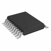
AD7328BRUZ Analog Devices Inc, AD7328BRUZ Datasheet - Page 32

AD7328BRUZ
Manufacturer Part Number
AD7328BRUZ
Description
IC ADC 12BIT+ SAR 8CHAN 20TSSOP
Manufacturer
Analog Devices Inc
Specifications of AD7328BRUZ
Data Interface
DSP, MICROWIRE™, QSPI™, Serial, SPI™
Design Resources
Using AD7328 in Appls with Single-Ended Industrial-Level Signals (CN0047)
Number Of Bits
12
Sampling Rate (per Second)
1M
Number Of Converters
1
Power Dissipation (max)
30mW
Voltage Supply Source
Dual ±
Operating Temperature
-40°C ~ 85°C
Mounting Type
Surface Mount
Package / Case
20-TSSOP (0.173", 4.40mm Width)
Resolution (bits)
13bit
Sampling Rate
1MSPS
Input Channel Type
Pseudo Differential, Single Ended
Supply Current
900µA
Digital Ic Case Style
TSSOP
No. Of Pins
20
Lead Free Status / RoHS Status
Lead free / RoHS Compliant
For Use With
EVAL-AD7328CBZ - BOARD EVALUATION FOR AD7328
Lead Free Status / Rohs Status
RoHS Compliant part
Electrostatic Device
Available stocks
Company
Part Number
Manufacturer
Quantity
Price
Part Number:
AD7328BRUZ
Manufacturer:
ADI/亚德诺
Quantity:
20 000
Company:
Part Number:
AD7328BRUZ-REEL7
Manufacturer:
ALLEGRO
Quantity:
1 200
AD7328
MICROPROCESSOR INTERFACING
The serial interface on the AD7328 allows the part to be directly
connected to a range of different microprocessors. This section
explains how to interface the AD7328 with some common
microcontroller and DSP serial interface protocols.
AD7328 TO ADSP-21xx
The ADSP-21xx family of DSPs interfaces directly to the AD7328
without requiring glue logic. The V
the same supply voltage as that of the ADSP-21xx. This allows
the ADC to operate at a higher supply voltage than its serial inter-
face. The SPORT0 on the ADSP-21xx should be configured as
shown in Table 14.
Table 14. SPORT0 Control Register Setup
Setting
TFSW = RFSW = 1
INVRFS = INVTFS = 1
DTYPE = 00
SLEN = 1111
ISCLK = 1
TFSR = RFSR = 1
IRFS = 0
ITFS = 1
The connection diagram is shown in Figure 54. The ADSP-21xx
has TFS0 and RFS0 tied together. TFS0 is set as an output, and
RFS0 is set as an input. The DSP operates in alternative framing
mode, and the SPORT0 control register is set up as described in
Table 14. The frame synchronization signal generated on TFS is
tied to CS and, as with all signal processing applications, requires
equidistant sampling. However, as in this example, the timer
interrupt is used to control the sampling rate of the ADC, and
under certain conditions equidistant sampling cannot be achieved.
The timer registers are loaded with a value that provides an
interrupt at the required sampling interval. When an interrupt
is received, a value is transmitted with TFS/DT (ADC control
word). The TFS is used to control the RFS and, hence, the reading
of data.
1
ADDITIONAL PINS OMITTED FOR CLARITY.
V
DRIVE
AD7328
Figure 54. Interfacing the AD7328 to the ADSP-21xx
DOUT
SCLK
1
DIN
CS
Description
Alternative framing
Active low frame signal
Right justify data
16-bit data-word
Internal serial clock
Frame every word
Internal receive frame sync
Internal transmit frame sync
DRIVE
pin of the AD7328 takes
SCLK0
TFS0
RFS0
DT0
DR0
ADSP-21xx
V
DD
1
Rev. B | Page 32 of 36
The frequency of the serial clock is set in the SCLKDIV register.
When the instruction to transmit with TFS is given (AX0 = TX0),
the state of the serial clock is checked. The DSP waits until the
SCLK has gone high, low, and high again before starting the trans-
mission. If the timer and SCLK are chosen so that the instruction
to transmit occurs on or near the rising edge of SCLK, data can
be transmitted immediately or at the next clock edge.
For example, if the ADSP-21xx has a master clock frequency of
16 MHz and the SCLKDIV register is loaded with the value 3,
an SCLK of 2 MHz is obtained, and eight master clock periods
elapse for every one SCLK period. If the timer registers are loaded
with the value 803, 100.5 SCLKs occur between interrupts and,
subsequently, between transmit instructions. This situation leads
to nonequidistant sampling because the transmit instruction occurs
on an SCLK edge. If the number of SCLKs between interrupts is
an integer of N, equidistant sampling is implemented by the DSP.
AD7328 TO ADSP-BF53x
The ADSP-BF53x family of DSPs interfaces directly to the
AD7328 without requiring glue logic, as shown in Figure 55.
The SPORT0 Receive Configuration 1 register should be set up
as outlined in Table 15.
Table 15. SPORT0 Receive Configuration 1 Register
Setting
RCKFE = 1
LRFS = 1
RFSR = 1
IRFS = 1
RLSBIT = 0
RDTYPE = 00
IRCLK = 1
RSPEN = 1
SLEN = 1111
TFSR = RFSR = 1
1
ADDITIONAL PINS OMITTED FOR CLARITY.
V
DRIVE
Figure 55. Interfacing the AD7328 to the ADSP-BF53x
AD7328
DOUT
SCLK
1
DIN
CS
Internal receive clock
Description
Sample data with falling edge of RSCLK
Active low frame signal
Frame every word
Internal RFS used
Receive MSB first
Zero fill
Receive enable
16-bit data-word
Transmit and receive frame sync
RSCLK0
RFS0
DT0
DR0
ADSP-BF53x
V
DD
1


