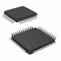
ADC10D020CIVS/NOPB National Semiconductor, ADC10D020CIVS/NOPB Datasheet - Page 3

ADC10D020CIVS/NOPB
Manufacturer Part Number
ADC10D020CIVS/NOPB
Description
IC ADC 10BIT 48-TQFP
Manufacturer
National Semiconductor
Datasheet
1.ADC10D020CIVSNOPB.pdf
(32 pages)
Specifications of ADC10D020CIVS/NOPB
Number Of Bits
10
Sampling Rate (per Second)
20M
Number Of Converters
2
Power Dissipation (max)
150mW
Voltage Supply Source
Analog and Digital
Operating Temperature
-40°C ~ 85°C
Mounting Type
Surface Mount
Package / Case
48-VFQFP
Number Of Elements
2
Resolution
10Bit
Architecture
Pipelined
Sample Rate
20MSPS
Input Polarity
Bipolar
Input Type
Voltage
Rated Input Volt
±0.5/±1V
Differential Input
Yes
Power Supply Requirement
Analog and Digital
Single Supply Voltage (typ)
3V
Single Supply Voltage (min)
2.7V
Single Supply Voltage (max)
3.6V
Dual Supply Voltage (typ)
Not RequiredV
Dual Supply Voltage (min)
Not RequiredV
Dual Supply Voltage (max)
Not RequiredV
Differential Linearity Error
-1LSB/1.2LSB
Integral Nonlinearity Error
±1.8LSB
Operating Temp Range
-40C to 85C
Operating Temperature Classification
Industrial
Mounting
Surface Mount
Pin Count
48
Package Type
TQFP
Input Signal Type
Differential
Lead Free Status / RoHS Status
Lead free / RoHS Compliant
Other names
*ADC10D020CIVS
*ADC10D020CIVS/NOPB
ADC10D020CIVS
*ADC10D020CIVS/NOPB
ADC10D020CIVS
Available stocks
Company
Part Number
Manufacturer
Quantity
Price
Company:
Part Number:
ADC10D020CIVS/NOPB
Manufacturer:
Texas Instruments
Quantity:
10 000
Pin Descriptions and Equivalent Circuits
Pin No.
48
47
37
38
45
43
44
1
Symbol
V
V
V
V
Q+
Q−
CMO
I+
I−
REF
RP
RN
Equivalent Circuit
3
Analog inputs to “I” ADC. Nominal conversion range is 1.25V to
1.75V with GAIN pin low, or 1.0V to 2.0V with GAIN pin high.
Analog inputs to “Q” ADC. Nominal conversion range is 1.25V to
1.75V with GAIN pin low, or 1.0V to 2.0V with GAIN pin high.
Analog Reference Voltage input. The voltage at this pin should be
in the range of 0.8V to 1.5V. With 1.0V at this pin and the GAIN pin
low, the full scale differential inputs are 1 V
and the GAIN pin high, the full scale differential inputs are 2 V
This pin should be bypassed with a minimum 1 µF capacitor.
This is an analog output which can be used as a reference source
and/or to set the common mode voltage of the input. It should be
bypassed with a minimum of 1 µF low ESR capacitor in parallel with
a 0.1 µF capacitor. This pin has a nominal output voltage of 1.5V
and has a 1 mA output source capability.
Top of the reference ladder. Do not drive this pin. Bypass this pin
with a 10 µF low ESR capacitor and a 0.1 µF capacitor.
Bottom of the reference ladder. Do not drive this pin. Bypass this
pin with a 10 µF low ESR capacitor and a 0.1 µF capacitor.
Description
P-P
. With 1.0V at this pin
www.national.com
P-P
.


