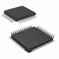
ADC10D020CIVS/NOPB National Semiconductor, ADC10D020CIVS/NOPB Datasheet - Page 8

ADC10D020CIVS/NOPB
Manufacturer Part Number
ADC10D020CIVS/NOPB
Description
IC ADC 10BIT 48-TQFP
Manufacturer
National Semiconductor
Datasheet
1.ADC10D020CIVSNOPB.pdf
(32 pages)
Specifications of ADC10D020CIVS/NOPB
Number Of Bits
10
Sampling Rate (per Second)
20M
Number Of Converters
2
Power Dissipation (max)
150mW
Voltage Supply Source
Analog and Digital
Operating Temperature
-40°C ~ 85°C
Mounting Type
Surface Mount
Package / Case
48-VFQFP
Number Of Elements
2
Resolution
10Bit
Architecture
Pipelined
Sample Rate
20MSPS
Input Polarity
Bipolar
Input Type
Voltage
Rated Input Volt
±0.5/±1V
Differential Input
Yes
Power Supply Requirement
Analog and Digital
Single Supply Voltage (typ)
3V
Single Supply Voltage (min)
2.7V
Single Supply Voltage (max)
3.6V
Dual Supply Voltage (typ)
Not RequiredV
Dual Supply Voltage (min)
Not RequiredV
Dual Supply Voltage (max)
Not RequiredV
Differential Linearity Error
-1LSB/1.2LSB
Integral Nonlinearity Error
±1.8LSB
Operating Temp Range
-40C to 85C
Operating Temperature Classification
Industrial
Mounting
Surface Mount
Pin Count
48
Package Type
TQFP
Input Signal Type
Differential
Lead Free Status / RoHS Status
Lead free / RoHS Compliant
Other names
*ADC10D020CIVS
*ADC10D020CIVS/NOPB
ADC10D020CIVS
*ADC10D020CIVS/NOPB
ADC10D020CIVS
Available stocks
Company
Part Number
Manufacturer
Quantity
Price
Company:
Part Number:
ADC10D020CIVS/NOPB
Manufacturer:
Texas Instruments
Quantity:
10 000
www.national.com
Symbol
POWER SUPPLY CHARACTERISTICS
I
I
PWR
PSRR1 Power Supply Rejection Ratio
PSRR2 Power Supply Rejection Ratio
f
f
t
t
t
t
t
t
t
t
t
t
Symbol
A
DR
CLK
CLK
r
OC
OD
DIQ
SKEW
AD
AJ
VALID
WUPD
WUSB
, t
AC Electrical Characteristics OS = Low (Multiplexed Mode)
The following specifications apply for V
FSR = 1.0 V
for T
+ I
f
1
2
D
A
= T
Core Supply Current
Digital Output Driver Supply Current
(Note
Power Consumption
Maximum Clock Frequency
Minimum Clock Frequency
Duty Cycle
Pipeline Delay (Latency)
Output Rise and Fall Times
Offset Correction Pulse Width
Output Delay from CLK Edge to Data
Valid
I/Q Output Delay
I/Q to Data Delay
Sampling (Aperture) Delay
Aperture Jitter
Data Valid Time
Overrange Recovery Time
PD Low to 1/2 LSB Accurate Conversion
(Wake-Up Time)
STBY Low to 1/2 LSB Accurate
Conversion (Wake-Up Time)
MIN
P-P
10)
to T
, C
I Data
Q Data
L
MAX
= 15 pF, f
Parameter
: all other limits T
Parameter
CLK
= 20 MHz, 50% Duty Cycle, R
A
A
= 25°C
= V
D
PD = LOW, STBY = LOW, dc input
PD = LOW, STBY = HIGH
PD = HIGH, STBY = LOW or HIGH
PD = LOW, STBY = LOW, dc input
PD = LOW, STBY = HIGH
PD = HIGH, STBY = LOW or HIGH
PD = LOW, STBY = LOW, dc input
PD = LOW, STBY = LOW, 1 MHz Input
PD = LOW, STBY = HIGH
PD = HIGH, STBY = LOW or HIGH
Change in Full Scale with 2.7V to 3.6V Supply
Change
Rejection at output with 20 MHz, 250 mV
Riding on V
= V
(Note
DR
Differential V
= +3.0V
7)
A
and V
DC
S
, V
= 50Ω, t
IN
8
Conditions
Conditions
D
REF
step from 1.5V to 0V
= 1.0 V
rc
= t
fc
DC
< 4 ns, NOT offset corrected. Boldface limits apply
, GAIN = OF = 0V, OS = 0V, V
P-P
(Note
Typical
±200
<10
800
2.4
30
50
13
13
21
50
<1
(Note
Typical
1
4
47.6
0.22
150
178
8.8
1.3
0.1
0.1
27
<1
90
52
8)
8)
(Note
Limits
(Note
2.5
3.0
Limits
20
30
70
10
18
169
IN
1.4
55
9)
(a.c. coupled) =
9)
Clock Cycles
Clock Cycles
MHz (min)
mW (max)
ns (max)
mA (max)
mA (max)
% (max)
ps (rms)
(Limits)
ns (min)
% (min)
(Limits)
Units
MHz
Units
ms
mW
mW
mW
ns
ns
ps
ns
ns
ns
ns
mA
mA
mA
mA
dB
dB


