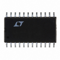
LTC1273BCSW Linear Technology, LTC1273BCSW Datasheet - Page 16

LTC1273BCSW
Manufacturer Part Number
LTC1273BCSW
Description
IC A/D CONV 12BIT SAMPLNG 24SOIC
Manufacturer
Linear Technology
Specifications of LTC1273BCSW
Number Of Bits
12
Sampling Rate (per Second)
300k
Data Interface
Parallel
Number Of Converters
1
Power Dissipation (max)
75mW
Voltage Supply Source
Single Supply
Operating Temperature
0°C ~ 70°C
Mounting Type
Surface Mount
Package / Case
24-SOIC (0.300", 7.50mm Width)
Lead Free Status / RoHS Status
Contains lead / RoHS non-compliant
Other names
LTC1273BCS
Available stocks
Company
Part Number
Manufacturer
Quantity
Price
Part Number:
LTC1273BCSW
Manufacturer:
LT/凌特
Quantity:
20 000
Company:
Part Number:
LTC1273BCSW#PBF
Manufacturer:
LT
Quantity:
352
Part Number:
LTC1273BCSW#PBF
Manufacturer:
LINEAR/凌特
Quantity:
20 000
Part Number:
LTC1273BCSW#TRPBF
Manufacturer:
LINEAR/凌特
Quantity:
20 000
LTC1273
LTC1275/LTC1276
A
on all three inputs to initiate a conversion. Once initiated it
cannot be restarted until the conversion is complete.
Converter status is indicated by the BUSY output, and this
is low while conversion is in progress.
There are two modes of operation as outlined by the timing
diagrams of Figures 13 to 16. Slow Memory Mode is
designed for microprocessors which can be driven into a
WAIT state. A READ operation brings CS and RD low which
initiates a conversion and data is read when conversion is
complete. The second is the ROM Mode which does not
require microprocessor WAIT states. A READ operation
brings CS and RD low which initiates a conversion and
reads the previous conversion result.
Data Format
The output format can be either a complete parallel load for
16-bit microprocessors or a two byte load for 8-bit micro-
processors. Data is always right justified (i.e., LSB is the
most right-hand bit in a 16-bit word). For a two byte read,
only data outputs D7...D0/8 are used. Byte selection is
governed by the HBEN input which controls an internal
digital multiplexer. This multiplexes the 12-bits of conver-
sion data onto the lower D7...D0/8 outputs (4MSBs or
16
Table 2. Slow Memory Mode, Parallel Read Data Bus Status
Data Outputs
Read
PPLICATI
DB11
D11
O
U
S
DB10
TRACK
D10
HOLD
BUSY
DATA
I FOR ATIO
RD
RD
CS
U
Figure 13. Slow Memory Mode, Parallel Read Timing Diagram
t
1
DB9
D9
t
t
t
3
12
2
W
DB8
D8
OLD DATA
DB11-DB0
t
CONV
U
DB7
D7
t
6
DB6
D6
8MSBs) where it can be read in two read cycles. The
4MSBs always appear on D11...D8 whenever the three-
state output drivers are turned on.
Slow Memory Mode, Parallel Read (HBEN = LOW)
Figure 13 and Table 2 show the timing diagram and data
bus status for Slow Memory Mode, Parallel Read. CS and
RD going low trigger a conversion and the ADC acknowl-
edges by taking BUSY low. Data from the previous conver-
sion appears on the three-state data outputs. BUSY re-
turns high at the end of conversion when the output
latches have been updated and the conversion result is
placed on data outputs D11...D0/8.
Slow Memory Mode, Two Byte Read
For a two byte read, only 8 data outputs D7...D0/8 are used.
Conversion start procedure and data output status for the
first read operation are identical to Slow Memory Mode,
Parallel Read. See Figure 14 timing diagram and Table 3
data bus status. At the end of the conversion, the low data
byte (D7...D0/8) is read from the ADC. A second READ
operation, with the HBEN high, places the high byte on data
outputs D3/11...D0/8 and disables conversion start. Note
NEW DATA
DB11-DB0
t
t
5
7
DB5
D5
t
11
t
10
DB4
D4
LTC1273/75/76 • F13
t
D3/11
1
DB3
D2/10
DB2
D1/9
DB1
127356fa
D0/8
DB0


