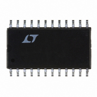
LTC1273BCSW Linear Technology, LTC1273BCSW Datasheet - Page 20

LTC1273BCSW
Manufacturer Part Number
LTC1273BCSW
Description
IC A/D CONV 12BIT SAMPLNG 24SOIC
Manufacturer
Linear Technology
Specifications of LTC1273BCSW
Number Of Bits
12
Sampling Rate (per Second)
300k
Data Interface
Parallel
Number Of Converters
1
Power Dissipation (max)
75mW
Voltage Supply Source
Single Supply
Operating Temperature
0°C ~ 70°C
Mounting Type
Surface Mount
Package / Case
24-SOIC (0.300", 7.50mm Width)
Lead Free Status / RoHS Status
Contains lead / RoHS non-compliant
Other names
LTC1273BCS
Available stocks
Company
Part Number
Manufacturer
Quantity
Price
Part Number:
LTC1273BCSW
Manufacturer:
LT/凌特
Quantity:
20 000
Company:
Part Number:
LTC1273BCSW#PBF
Manufacturer:
LT
Quantity:
352
Part Number:
LTC1273BCSW#PBF
Manufacturer:
LINEAR/凌特
Quantity:
20 000
Part Number:
LTC1273BCSW#TRPBF
Manufacturer:
LINEAR/凌特
Quantity:
20 000
LTC1273
LTC1275/LTC1276
A
This is a two byte read instruction which loads the ADC
data (address B000) into the HL register pair. During the
first read operation, BUSY forces the microprocessor to
WAIT for the LTC1273 conversion. No WAIT states are
inserted during the second read operation when the mi-
croprocessor is reading the high data byte.
TMS32010 Microcomputer
Figure 20 shows an LTC1273/TMS32010 interface. The
LTC1273 is operating in the ROM Mode.
The LTC1273 is mapped at a port address. The following
I/O instruction starts a conversion and reads the previous
conversion result into data memory.
When conversion is complete, a second I/O instruction
reads the up-to-date data into memory and starts another
conversion. A delay at least as long as the ADC conversion
time must be allowed between I/O instructions.
MUXing with CD4051
The high input impedance of the LTC1273/LTC1275/
LTC1276 provides an easy, cheap, fast, and accurate way
to multiplex many channels of data through one con-
verter. Figure 21 shows a low cost CD4051 connected to
the LTC1275. The LTC1275’s input draws no DC input
20
PPLICATI
LINEAR CIRCUITRY OMITTED FOR CLARITY
TMS32010
IN A,PA
DEN
PA2
PA0
D11
D0
Figure 20. TMS32010 Interface
O
U
PORT ADDRESS BUS
S
EN
(PA = PORT ADDRESS)
DATA BUS
I FOR ATIO
U
ADDRESS
DECODE
W
CS
RD
D11
D0/8
LTC1273/75/76
LTC1273/75/76 • F20
U
HBEN
CHANNELS
current so it can be accurately driven by the unbuffered
MUX. The CD4520 counter increments the MUX channel
after each sample is taken. Figure 22 shows the acquisi-
tion time of LTC1275 vs the source resistance. For a
500Ω maximum “on” resistance of the CD4051, the
acquisition time of the ADC is not greatly affected. For
larger source resistances, modest increases in acquisi-
tion time must be allowed.
8 INPUT
VARIES
Figure 22. Acqusition Time of LTC1275 vs Source Resistance
INPUT
±2.8V
CD4051
Figure 21. MUXing the LTC1275 with CD4051
–5V
V
V
EE
SS
4
3
2
1
0
10
V
A B C
5V
DD
R
SOURCE
V
IN
SOURCE RESISTANCE (Ω)
REQUIRED
BUFFER
100
A
NO
IN
500Ω
LTC1275
Q2
Q1
Q0
LTC1275
A
IN
5V
COUNTER
CD4520
RESET
1k
ENABLE
BUSY
LTC1273/75/76 • F22
D11
RD
D0
CS
•
•
•
10k
LTC1273/75/76 • F21
DSP
µP
OR
127356fa


