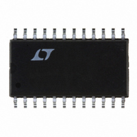
LTC1273BCSW Linear Technology, LTC1273BCSW Datasheet - Page 8

LTC1273BCSW
Manufacturer Part Number
LTC1273BCSW
Description
IC A/D CONV 12BIT SAMPLNG 24SOIC
Manufacturer
Linear Technology
Specifications of LTC1273BCSW
Number Of Bits
12
Sampling Rate (per Second)
300k
Data Interface
Parallel
Number Of Converters
1
Power Dissipation (max)
75mW
Voltage Supply Source
Single Supply
Operating Temperature
0°C ~ 70°C
Mounting Type
Surface Mount
Package / Case
24-SOIC (0.300", 7.50mm Width)
Lead Free Status / RoHS Status
Contains lead / RoHS non-compliant
Other names
LTC1273BCS
Available stocks
Company
Part Number
Manufacturer
Quantity
Price
Part Number:
LTC1273BCSW
Manufacturer:
LT/凌特
Quantity:
20 000
Company:
Part Number:
LTC1273BCSW#PBF
Manufacturer:
LT
Quantity:
352
Part Number:
LTC1273BCSW#PBF
Manufacturer:
LINEAR/凌特
Quantity:
20 000
Part Number:
LTC1273BCSW#TRPBF
Manufacturer:
LINEAR/凌特
Quantity:
20 000
PI FU CTIO S
TYPICAL PERFOR
LTC1273
LTC1275/LTC1276
A
(LTC1275) or ±5V (LTC1276).
V
AGND (10µF tantalum in parallel with 0.1µF ceramic).
AGND (Pin 3): Analog Ground.
D11-D4 (Pins 4 to 11): Three-State Data Outputs.
DGND (Pin 12): Digital Ground.
D3/11-D0/8 (Pins 13 to 16): Three-State Data Outputs.
NC (Pins 17 and 18): No Connection.
8
–100
–120
IN
REF
–40
–60
–20
–80
U
0
(Pin 1): Analog Input. 0V to 5V (LTC1273), ±2.5V
0
Intermodulation Distortion Plot
(Pin 2): +2.42V Reference Output. Bypass to
20
U
40
FREQUENCY (kHz)
60
–100
–10
–20
–30
–40
–50
–60
–70
–80
–90
80
0
10k
U
Spurious Free Dynamic Range
vs Input Frequency
f
f
f
SAMPLE
IN1
IN2
f
100
SAMPLE
= 29.37kHz
= 32.446kHz
120
= 300kHz
W
LTC1273/75/76 • F05
= 300kHz
INPUT FREQUENCY (Hz)
100k
140
A
U
160
CE
1M
C
LTC1273/75/76 • TPC12
4500
4000
3500
3000
2500
2000
1500
1000
HARA TERISTICS
500
0
10
Acquisition Time
vs Source Impedance
10M
C
100
R
SOURCE
HBEN (Pin 19): High Byte Enable Input. This pin is used
to multiplex the internal 12-bit conversion result into
the lower bit outputs (D7-D0/8). See Table 1. HBEN also
disables conversion start when HIGH.
RD (Pin 20): READ Input. This active low signal starts
a conversion when CS and HBEN are low. RD also
enables the output drivers when CS is low.
CS (Pin 21): The CHIP SELECT Input must be low for
the ADC to recognize RD and HBEN inputs.
BUSY (Pin 22): The BUSY Output shows the converter
status. It is low when a conversion is in progress.
(Ω)
1k
LTC1273/75/76 • TPC10
2.435
2.430
2.425
2.420
2.415
2.410
2.405
– 5
Reference Voltage
vs Load Current
10k
– 4
–3
LOAD CURRENT (mA)
–2
80
70
60
50
40
30
20
10
0
1k
S/(N + D) vs Input Frequency and
Amplitude
–1
LTC1273/75/76 • TPC13
0
10k
INPUT FREQUENCY (Hz)
V
V
V
IN
IN
IN
1
= –20dB
= –60dB
= 0dB
100k
2
f
SAMPLE
LTC1273/75/76 • TPC11
1M
= 300kHz
127356fa
10M


