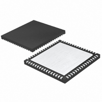
LTC2208CUP-14 Linear Technology, LTC2208CUP-14 Datasheet - Page 21

LTC2208CUP-14
Manufacturer Part Number
LTC2208CUP-14
Description
IC ADC 14BIT 130MSPS 64-QFN
Manufacturer
Linear Technology
Datasheet
1.LTC2208CUP-14TR.pdf
(28 pages)
Specifications of LTC2208CUP-14
Number Of Bits
14
Sampling Rate (per Second)
130M
Data Interface
Parallel
Number Of Converters
1
Power Dissipation (max)
1.78W
Voltage Supply Source
Single Supply
Operating Temperature
0°C ~ 70°C
Mounting Type
Surface Mount
Package / Case
64-WFQFN, Exposed Pad
Lead Free Status / RoHS Status
Contains lead / RoHS non-compliant
APPLICATIONS INFORMATION
The internal programmable gain amplifi er provides the
internal reference voltage for the ADC. This amplifi er has
very stringent settling requirements and is not accessible
for external use.
The SENSE pin can be driven ±5% around the nominal 2.5V
or 1.25V external reference inputs. This adjustment range
can be used to trim the ADC gain error or other system
gain errors. When selecting the internal reference, the
SENSE pin should be tied to V
as possible. If the sense pin is driven externally it should
be bypassed to ground as close to the device as possible
with 1μF ceramic capacitor.
PGA Pin
The PGA pin selects between two gain settings for the ADC
front-end. PGA = 0 selects an input range of 2.25V
PGA = 1 selects an input range of 1.5V
range has the best SNR; however, the distortion will be
higher for input frequencies above 100MHz. For applica-
tions with high input frequencies, the low input range
will have improved distortion; however, the SNR will be
approximately 1.8dB worse. See the Typical Performance
Characteristics section.
Driving the Encode Inputs
The noise performance of the LTC2208-14 can depend on
the encode signal quality as much as on the analog input.
The encode inputs are intended to be driven differentially,
primarily for noise immunity from common mode noise
sources. Each input is biased through a 6k resistor to a
1.6V bias. The bias resistors set the DC operating point
for transformer coupled drive circuits and can set the logic
threshold for single-ended drive circuits.
Any noise present on the encode signal will result in ad-
ditional aperture jitter that will be RMS summed with the
inherent ADC aperture jitter.
Figure 7. A 2.25V Range ADC with an External 2.5V Reference
3.3V
1μF
2
LT1461-2.5
1.25V
4
6
DD
as close to the converter
SENSE
2.2μF
2.2μF
V
CM
P-P
LTC2208-14
. The 2.25V input
220814 F07
P-P
;
In applications where jitter is critical (high input frequen-
cies), take the following into consideration:
1. Differential drive should be used.
2. Use as large an amplitude possible. If using trans-
3. If the ADC is clocked with a fi xed frequency sinusoidal
4. Balance the capacitance and series resistance at both
The encode inputs have a common mode range of 1.2V
to 3V. Each input may be driven from ground to V
single-ended drive.
former coupling, use a higher turns ratio to increase the
amplitude.
signal, fi lter the encode signal to reduce wideband
noise.
encode inputs such that any coupled noise will appear
at both inputs as common mode noise.
ENC
ENC –
T1 = MA/COM ETC1-1-13
RESISTORS AND CAPACITORS
ARE 0402 PACKAGE SIZE
Figure 8a. Equivalent Encode Input Circuit
+
0.1μF
0.1μF
Figure 8b. Transformer Driven Encode
LTC2208-14
V
DD
T1
50Ω
50Ω
V
DD
1.6V
6k
1.6V
6k
V
0.1μF
DD
100Ω
8.2pF
LTC2208-14
ENC –
ENC
+
LTC2208-14
TO INTERNAL
ADC CLOCK
DRIVERS
220814 F08b
220814 F08a
21
DD
220814fb
for


