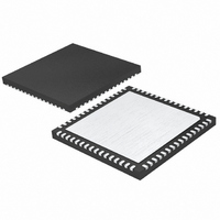
LTC2208CUP-14 Linear Technology, LTC2208CUP-14 Datasheet - Page 22

LTC2208CUP-14
Manufacturer Part Number
LTC2208CUP-14
Description
IC ADC 14BIT 130MSPS 64-QFN
Manufacturer
Linear Technology
Datasheet
1.LTC2208CUP-14TR.pdf
(28 pages)
Specifications of LTC2208CUP-14
Number Of Bits
14
Sampling Rate (per Second)
130M
Data Interface
Parallel
Number Of Converters
1
Power Dissipation (max)
1.78W
Voltage Supply Source
Single Supply
Operating Temperature
0°C ~ 70°C
Mounting Type
Surface Mount
Package / Case
64-WFQFN, Exposed Pad
Lead Free Status / RoHS Status
Contains lead / RoHS non-compliant
LTC2208-14
APPLICATIONS INFORMATION
Maximum and Minimum Encode Rates
The maximum encode rate for the LTC2208-14 is 130Msps.
For the ADC to operate properly the encode signal should
have a 50% (±5%) duty cycle. Each half cycle must have at
least 3.65ns for the ADC internal circuitry to have enough
settling time for proper operation. Achieving a precise 50%
duty cycle is easy with differential sinusoidal drive using
a transformer or using symmetric differential logic such
as PECL or LVDS. When using a single-ended ENCODE
signal asymmetric rise and fall times can result in duty
cycles that are far from 50%.
An optional clock duty cycle stabilizer can be used if the
input clock does not have a 50% duty cycle. This circuit
uses the rising edge of ENC pin to sample the analog input.
The falling edge of ENC is ignored and an internal falling
edge is generated by a phase-locked loop. The input clock
duty cycle can vary from 30% to 70% and the clock duty
cycle stabilizer will maintain a constant 50% internal duty
cycle. If the clock is turned off for a long period of time,
the duty cycle stabilizer circuit will require one hundred
clock cycles for the PLL to lock onto the input clock. To
use the clock duty cycle stabilizer, the MODE pin must be
connected to 1/3V
22
Figure 10. ENC Drive Using a CMOS to PECL Translator
MC100LVELT22
V
THRESHOLD
Figure 9. Single-Ended ENC Drive,
Not Recommended for Low Jitter
D0
DD
= 1.6V
3.3V
or 2/3V
Q0
Q0
0.1μF
130Ω
83Ω
1.6V
DD
3.3V
using external resistors.
ENC
ENC
130Ω
83Ω
+
–
ENC
ENC
LTC2208-14
+
–
LTC2208-14
220814 F09
220814 F10
The lower limit of the LTC2208-14 sample rate is determined
by droop of the sample and hold circuits. The pipelined
architecture of this ADC relies on storing analog signals on
small valued capacitors. Junction leakage will discharge
the capacitors. The specifi ed minimum operating frequency
for the LTC2208-14 is 1Msps.
DIGITAL OUTPUTS
Digital Output Modes
The LTC2208-14 can operate in four digital output modes:
standard LVDS, low power LVDS, full rate CMOS, and
demultiplexed CMOS. The LVDS pin selects the mode of
operation. This pin has a four level logic input, centered at
0, 1/3V
be used to set the 1/3V
shows the logic states for the LVDS pin.
Table 1. LVDS Pin Function
LVDS
0V(GND)
1/3V
2/3V
V
Digital Output Buffers (CMOS Modes)
Figure 11 shows an equivalent circuit for a single output
buffer in CMOS Mode, Full-Rate or Demultiplexed. Each
buffer is powered by OV
ADC power and ground. The additional N-channel transistor
in the output driver allows operation down to low voltages.
The internal resistor in series with the output makes the
output appear as 50Ω to external circuitry and eliminates
the need for external damping resistors.
As with all high speed/high resolution converters, the
digital output loading can affect the performance. The
digital outputs of the LTC2208-14 should drive a minimum
capacitive load to avoid possible interaction between the
digital outputs and sensitive input circuitry. The output
should be buffered with a device such as a ALVCH16373
CMOS latch. For full speed operation the capacitive load
should be kept under 10pF . A resistor in series with the
DD
DD
DD
DD
, 2/3V
DD
and V
DD
DD
DD
. An external resistor divider can
and 2/3V
and OGND, isolated from the
DIGITAL OUTPUT MODE
Full-Rate CMOS
Demultiplexed CMOS
Low Power LVDS
LVDS
DD
logic levels. Table 1
220814fb


