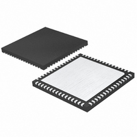
LTC2208CUP-14 Linear Technology, LTC2208CUP-14 Datasheet - Page 24

LTC2208CUP-14
Manufacturer Part Number
LTC2208CUP-14
Description
IC ADC 14BIT 130MSPS 64-QFN
Manufacturer
Linear Technology
Datasheet
1.LTC2208CUP-14TR.pdf
(28 pages)
Specifications of LTC2208CUP-14
Number Of Bits
14
Sampling Rate (per Second)
130M
Data Interface
Parallel
Number Of Converters
1
Power Dissipation (max)
1.78W
Voltage Supply Source
Single Supply
Operating Temperature
0°C ~ 70°C
Mounting Type
Surface Mount
Package / Case
64-WFQFN, Exposed Pad
Lead Free Status / RoHS Status
Contains lead / RoHS non-compliant
LTC2208-14
APPLICATIONS INFORMATION
Overfl ow Bit
An overfl ow output bit (OF) indicates when the converter is
overranged or underranged. In CMOS mode, a logic high
on the OFA pin indicates an overfl ow or underfl ow on the
A data bus, while a logic high on the OFB pin indicates
an overfl ow on the B data bus. In LVDS mode, a differen-
tial logic high on OF
underfl ow.
Output Clock
The ADC has a delayed version of the encode input avail-
able as a digital output, CLKOUT. The CLKOUT pin can
be used to synchronize the converter data to the digital
system. This is necessary when using a sinusoidal en-
code. In both CMOS modes, A bus data will be updated
as CLKOUTA falls and CLKOUTB rises. In demultiplexed
CMOS mode the B bus data will be updated as CLKOUTA
falls and CLKOUTB rises.
In Full Rate CMOS Mode, only the A data bus is active;
data may be latched on the rising edge of CLKOUTA or
the falling edge of CLKOUTB.
In demultiplexed CMOS mode CLKOUTA and CLKOUTB
will toggle at 1/2 the frequency of the encode signal. Both
the A bus and the B bus may be latched on the rising edge
of CLKOUTA or the falling edge of CLKOUTB.
Digital Output Randomizer
Interference from the ADC digital outputs is sometimes
unavoidable. Interference from the digital outputs may be
from capacitive or inductive coupling or coupling through
the ground plane. Even a tiny coupling factor can result in
discernible unwanted tones in the ADC output spectrum.
By randomizing the digital output before it is transmitted
off chip, these unwanted tones can be randomized, trading
a slight increase in the noise fl oor for a large reduction in
unwanted tone amplitude.
The digital output is “Randomized” by applying an exclu-
sive-OR logic operation between the LSB and all other data
output bits. To decode, the reverse operation is applied;
that is, an exclusive-OR operation is applied between the
24
+
/OF
–
pins indicates an overfl ow or
LSB and all other bits. The LSB, OF and CLKOUT outputs
are not affected. The output Randomizer function is active
when the RAND pin is high.
Output Driver Power
Separate output power and ground pins allow the output
drivers to be isolated from the analog circuitry. The power
supply for the digital output buffers, OV
to the same power supply as for the logic being driven.
For example, if the converter is driving a DSP powered
by a 1.8V supply, then OV
1.8V supply. In CMOS mode OV
any logic voltage up to the 3.6V. OGND can be powered
with any voltage from ground up to 1V and must be less
than OV
and OV
a 3.3V supply and OGND should be connected to GND.
RAND = HIGH,
RANDOMIZER
Figure 13. Functional Equivalent of Digital Output Randomizer
ENABLED
DD
DD
. In LVDS Mode, OV
. The logic outputs will swing between OGND
D0
RAND
CLKOUT
D13
D12
D2
D1
OF
DD
should be tied to that same
DD
DD
should be connected to
can be powered with
•
•
•
DD
220814 F13
, should be tied
CLKOUT
OF
D13/D0
D12/D0
D2/D0
D1/D0
D0
220814fb


