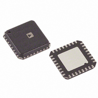
AD9237BCPZ-20 Analog Devices Inc, AD9237BCPZ-20 Datasheet - Page 16

AD9237BCPZ-20
Manufacturer Part Number
AD9237BCPZ-20
Description
IC ADC 12BIT SGL 20MSPS 32LFCSP
Manufacturer
Analog Devices Inc
Specifications of AD9237BCPZ-20
Data Interface
Parallel
Number Of Bits
12
Sampling Rate (per Second)
20M
Number Of Converters
3
Power Dissipation (max)
85mW
Voltage Supply Source
Single Supply
Operating Temperature
-40°C ~ 85°C
Mounting Type
Surface Mount
Package / Case
32-VFQFN, CSP Exposed Pad
Resolution (bits)
12bit
Input Channel Type
Differential
Supply Voltage Range - Analogue
2.7V To 3.6V
Supply Voltage Range - Digital
2.25V To 3.6V
Supply Current
30.5mA
Sampling Rate
20MSPS
Rohs Compliant
Yes
Lead Free Status / RoHS Status
Lead free / RoHS Compliant
Available stocks
Company
Part Number
Manufacturer
Quantity
Price
Company:
Part Number:
AD9237BCPZ-20
Manufacturer:
INFINEON
Quantity:
2 300
Part Number:
AD9237BCPZ-20
Manufacturer:
ADI/亚德诺
Quantity:
20 000
AD9237
APPLYING THE AD9237
THEORY OF OPERATION
The AD9237 uses a calibrated, 11-stage pipeline architecture
with a patented input SHA implemented. Each stage of the
pipeline, excluding the last, consists of a low resolution flash
ADC connected to a switched capacitor digital-to-analog
converter (DAC) and an interstage residue amplifier (MDAC).
The MDAC magnifies the difference between the reconstructed
DAC output and the flash input for the next stage in the
pipeline. One bit of redundancy is used in each stage to facilitate
digital correction of flash errors. The last stage consists of a
flash ADC.
The pipelined architecture permits the first stage to operate on a
new input sample, while the remaining stages operate on preceding
samples. While the converter captures a new input sample every
clock cycle, it takes eight clock cycles for the conversion to be
fully processed and to appear at the output, as shown in Figure 2.
The input stage contains a differential SHA that can be ac- or
dc-coupled in differential or single-ended modes. The output-
staging block aligns the data, carries out the error correction,
and passes the data to the output buffers. The output buffers
are powered from a separate supply, allowing adjustment of
the output voltage swing. During power-down and stand-by
operation, the output buffers go into a high impedance state.
The ADC samples the analog input on the rising edge of
the clock. System disturbances just prior to, or immediately
following, the rising edge of the clock and/or excessive clock
jitter can cause the SHA to acquire the wrong input value and
should be minimized.
ANALOG INPUT AND REFERENCE OVERVIEW
The analog input to the AD9237 is a differential switched
capacitor SHA that has been designed for optimum
performance while processing a differential input signal.
The SHA input can support a wide common-mode range
and maintain excellent performance, as shown in Figure 34.
An input common-mode voltage of midsupply minimizes
signal-dependant errors and provides optimum performance.
Figure 35 shows the clock signal alternately switching the
SHA between sample mode and hold mode. When the SHA is
switched into sample mode, the signal source must be capable
of charging the sample capacitors and settling within one-half
of a clock cycle. A small resistor in series with each input can
help reduce the peak transient current required from the output
stage of the driving source.
Rev. A | Page 16 of 24
In addition, a small shunt capacitor placed across the inputs
provides dynamic charging currents. This passive network
creates a low-pass filter at the ADC’s input; therefore, the
precise values are dependent on the application. In IF under-
sampling applications, the shunt capacitor(s) should be reduced
or removed depending on the input frequency. In combination
with the driving source impedance, the capacitors limit the
input bandwidth.
For best dynamic performance, the source impedances driving
VIN+ and VIN– should be matched so that common-mode
settling errors are symmetrical. These errors are reduced by the
common-mode rejection of the ADC.
An internal differential reference buffer creates positive and
negative reference voltages, REFT and REFB, that define the
span of the ADC core.
VIN+
VIN–
Figure 34. AD9237-65 SNR/SFDR vs. Input Common-Mode Level
90
80
70
60
50
40
30
C
C
PAR
PAR
0
Figure 35. Switched-Capacitor SHA Input
0.5
T
T
2.5MHz SFDR
INPUT COMMON-MODE LEVEL (V)
1.0
5pF
2.5MHz SNR
5pF
34.2MHz SFDR
34.2MHz SNR
1.5
T
T
2.0
2.5
H
H
3.0


