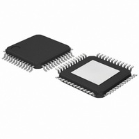
ADC1207S080HW/C1,5 NXP Semiconductors, ADC1207S080HW/C1,5 Datasheet - Page 12

ADC1207S080HW/C1,5
Manufacturer Part Number
ADC1207S080HW/C1,5
Description
IC ADC 12BIT 80MHZ SGL 48-HTQFP
Manufacturer
NXP Semiconductors
Datasheet
1.ADC1207S080HWC15.pdf
(21 pages)
Specifications of ADC1207S080HW/C1,5
Number Of Bits
12
Sampling Rate (per Second)
80M
Data Interface
Parallel
Number Of Converters
1
Power Dissipation (max)
990mW
Voltage Supply Source
Analog and Digital
Operating Temperature
-40°C ~ 85°C
Mounting Type
Surface Mount
Package / Case
48-TQFP Exposed Pad
Lead Free Status / RoHS Status
Lead free / RoHS Compliant
Other names
935286582518
Available stocks
Company
Part Number
Manufacturer
Quantity
Price
Company:
Part Number:
ADC1207S080HW/C1,5
Manufacturer:
NXP Semiconductors
Quantity:
10 000
NXP Semiconductors
ADC1207S080_2
Product data sheet
The ADC1207S080 generates an adjustable clock output called Complete Conversion
Signal (CCS), which can be used to control the acquisition of converted output data by the
digital circuit connected to the ADC1207S080 output data bus. Two logic inputs, DEL0 and
DEL1 pins, allow adjusting the delay of the edge of the CCS signal to achieve an optimal
position in the stable, usable zone of the data.
Table 8.
DEL1
0
0
1
1
Fig 6. Complete conversion signal timing diagram
(1) t
DEL0
0
1
0
1
d(CSS)
Complete conversion signal selection
D0 to D11
is referenced to the middle of the active data.
CCS output
high-impedance
active, typical delay 0.3 ns
active, typical delay 1.3 ns
active, typical delay 2.3 ns
CCS
Single 12 bits ADC, up to 80 MHz with direct/ultra high IF sampling
Rev. 02 — 7 August 2008
t
d(CCS)
(1)
ADC1207S080
014aaa433
© NXP B.V. 2008. All rights reserved.
12 of 21


