ADC1207S080HW/C1,5 NXP Semiconductors, ADC1207S080HW/C1,5 Datasheet - Page 9
ADC1207S080HW/C1,5
Manufacturer Part Number
ADC1207S080HW/C1,5
Description
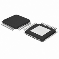
IC ADC 12BIT 80MHZ SGL 48-HTQFP
Manufacturer
NXP Semiconductors
Datasheet
1.ADC1207S080HWC15.pdf
(21 pages)
Specifications of ADC1207S080HW/C1,5
Number Of Bits
12
Sampling Rate (per Second)
80M
Data Interface
Parallel
Number Of Converters
1
Power Dissipation (max)
990mW
Voltage Supply Source
Analog and Digital
Operating Temperature
-40°C ~ 85°C
Mounting Type
Surface Mount
Package / Case
48-TQFP Exposed Pad
Lead Free Status / RoHS Status
Lead free / RoHS Compliant
Other names
935286582518
Available stocks
Company
Part Number
Manufacturer
Quantity
Price
Company:

Part Number:
ADC1207S080HW/C1,5
Manufacturer:
NXP Semiconductors
Quantity:
10 000


NXP Semiconductors
Table 5.
V
to +85 C; V
V
[1]
[2]
[3]
[4]
[5]
[6]
[7]
[8]
ADC1207S080_2
Product data sheet
Symbol
S/N
SFDR
ACPR
IMD2
IMD3
CCA
CCA
The circuit has two clock inputs: CLK and CLKN. There are 5 modes of operation:
a) PECL mode 1: (DC levels vary 1:1 with V
b) PECL mode 2: (DC levels vary 1:1 with V
c) PECL mode 3: (DC levels vary 1:1 with V
d) Differential AC driving mode 4: When driving the CLK input directly and with any AC signal of minimum 1 V (p-p) and with a DC level
e) TTL mode 5: CLK input is at TTL level and sampling is taken on the falling edge of the clock input signal. In that case CLKN pin has
Guaranteed by design.
The ADC input range can be adjusted with an external reference connected to pin FSIN. This voltage has to be referenced to V
Output data acquisition: the output data is available after the maximum delay of t
The 3 dB analog bandwidth is determined by the 3 dB reduction in the reconstructed output, the input being a full-scale sine wave.
The total harmonic distortion is obtained with the addition of the first five harmonics.
The signal-to-noise ratio takes into account all harmonics above five and noise up to Nyquist frequency.
Intermodulation measured relative to either tone with analog input frequencies f
amplitude and the total amplitude of both signals provides full-scale to the converter ( 6 dB below full-scale for each input signal). IMD3
is the ratio of the RMS value of either input tone to the RMS value of the worst case third order intermodulation product; IMD2 is the ratio
of the RMS value of either input tone to the RMS value of the worst case second order intermodulation product.
= 4.75 V to 5.25 V; V
= V
signal. A DC level of 3.65 V has to be applied on CLKN decoupled to GND via a 100 nF capacitor.
signal. A DC level of 3.65 V has to be applied on CLK decoupled to GND via a 100 nF capacitor.
of 2.5 V, the sampling takes place at the falling edge of the clock signal. When driving the CLKN input with the same signal, sampling
takes place at the rising edge of the clock signal. It is recommended to decouple the CLKN or CLK input to DGND via a 100 nF
capacitor.
to be connected to the ground.
CCD
Characteristics
i(IN)
Parameter
signal-to-noise ratio
spurious free dynamic
range
adjacent channel power
ratio
second-order
intermodulation
distortion
third-order
intermodulation
distortion
= 5 V, V
V
i(INN)
CCO
= 0.5 dBFS; V
= 3.3 V, T
CCD
…continued
= 4.75 V to 5.25 V; V
amb
Conditions
f
f
f
f
f
f
f
channel spacing;
B = 3.84 MHz
f
f
f
f
f
f
f
f
f
f
f
f
= 25 C and C
i
i
i
i
i
i
i
i
i
i
i
i
i
i
i
i
i
i
i
ref(fs)
1 = 21 MHz;
2 = 22 MHz
1 = 91.5 MHz;
2 = 94.5 MHz
1 = 174 MHz;
2 = 176 MHz
1 = 21 MHz;
2 = 22 MHz
1 = 91.5 MHz;
2 = 93.5 MHz
1 = 174 MHz;
2 = 176 MHz
= 21.4 MHz
= 93 MHz
= 175 MHz
= 21.4 MHz
= 93 MHz
= 175 MHz
= 93 MHz; 5 MHz
CCD
CCD
CCD
= V
Single 12 bits ADC, up to 80 MHz with direct/ultra high IF sampling
) CLKN input is at PECL level and sampling is taken on the rising edge of the clock input
) CLK input is at PECL level and sampling is taken on the falling edge of the clock input
) CLK and CLKN inputs are at differential PECL levels.
CCA
Rev. 02 — 7 August 2008
CCO
L
1.87 V; V
= 10 pF; unless otherwise specified.
= 2.7 V to 3.6 V; AGND and DGND shorted together; T
I(cm)
[7]
[8]
[8]
Min
-
63
-
-
68
-
-
-
-
-
-
-
-
= V
CCA
i
d(o)
1 and f
1.95 V; typical values measured at
.
Typ
67.4
67.2
66.5
76
78
74
70
i
89
86
83
88
82
83
2. The two input signals have the same
ADC1207S080
Max
-
-
-
-
-
-
-
-
-
-
-
-
-
© NXP B.V. 2008. All rights reserved.
amb
Unit
dBc
dBc
dBc
dBc
dBc
dBc
dB
dBFS
dBFS
dBFS
dBFS
dBFS
dBFS
= 40 C
CCA.
9 of 21
Related parts for ADC1207S080HW/C1,5
Image
Part Number
Description
Manufacturer
Datasheet
Request
R

Part Number:
Description:
Single 12 bits ADC
Manufacturer:
NXP Semiconductors
Datasheet:
Part Number:
Description:
NXP Semiconductors designed the LPC2420/2460 microcontroller around a 16-bit/32-bitARM7TDMI-S CPU core with real-time debug interfaces that include both JTAG andembedded trace
Manufacturer:
NXP Semiconductors
Datasheet:

Part Number:
Description:
NXP Semiconductors designed the LPC2458 microcontroller around a 16-bit/32-bitARM7TDMI-S CPU core with real-time debug interfaces that include both JTAG andembedded trace
Manufacturer:
NXP Semiconductors
Datasheet:
Part Number:
Description:
NXP Semiconductors designed the LPC2468 microcontroller around a 16-bit/32-bitARM7TDMI-S CPU core with real-time debug interfaces that include both JTAG andembedded trace
Manufacturer:
NXP Semiconductors
Datasheet:
Part Number:
Description:
NXP Semiconductors designed the LPC2470 microcontroller, powered by theARM7TDMI-S core, to be a highly integrated microcontroller for a wide range ofapplications that require advanced communications and high quality graphic displays
Manufacturer:
NXP Semiconductors
Datasheet:
Part Number:
Description:
NXP Semiconductors designed the LPC2478 microcontroller, powered by theARM7TDMI-S core, to be a highly integrated microcontroller for a wide range ofapplications that require advanced communications and high quality graphic displays
Manufacturer:
NXP Semiconductors
Datasheet:
Part Number:
Description:
The Philips Semiconductors XA (eXtended Architecture) family of 16-bit single-chip microcontrollers is powerful enough to easily handle the requirements of high performance embedded applications, yet inexpensive enough to compete in the market for hi
Manufacturer:
NXP Semiconductors
Datasheet:
Part Number:
Description:
The XA-S3 device is a member of Philips Semiconductors? XA(eXtended Architecture) family of high performance 16-bitsingle-chip microcontrollers
Manufacturer:
NXP Semiconductors
Datasheet:

Part Number:
Description:
The NXP BlueStreak LH75401/LH75411 family consists of two low-cost 16/32-bit System-on-Chip (SoC) devices
Manufacturer:
NXP Semiconductors
Datasheet:
Part Number:
Description:
The NXP LPC3130/3131 combine an 180 MHz ARM926EJ-S CPU core, high-speed USB2
Manufacturer:
NXP Semiconductors
Datasheet:
Part Number:
Description:
The NXP LPC3141 combine a 270 MHz ARM926EJ-S CPU core, High-speed USB 2
Manufacturer:
NXP Semiconductors
Part Number:
Description:
The NXP LPC3143 combine a 270 MHz ARM926EJ-S CPU core, High-speed USB 2
Manufacturer:
NXP Semiconductors

Part Number:
Description:
The NXP LPC3152 combines an 180 MHz ARM926EJ-S CPU core, High-speed USB 2
Manufacturer:
NXP Semiconductors