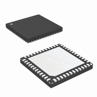
KAD5512P-25Q48 Intersil, KAD5512P-25Q48 Datasheet - Page 18

KAD5512P-25Q48
Manufacturer Part Number
KAD5512P-25Q48
Description
IC ADC 12BIT 250MSPS SGL 48-QFN
Manufacturer
Intersil
Series
FemtoCharge™r
Datasheet
1.KAD5512P-25Q72.pdf
(36 pages)
Specifications of KAD5512P-25Q48
Number Of Bits
12
Sampling Rate (per Second)
250M
Data Interface
Serial, SPI™
Number Of Converters
1
Power Dissipation (max)
286mW
Voltage Supply Source
Single Supply
Operating Temperature
-40°C ~ 85°C
Mounting Type
Surface Mount
Package / Case
48-VQFN
For Use With
KDC5512-Q48EVAL - DAUGHTER CARD FOR KAD5512KDC5512EVAL - DAUGHTER CARD FOR KAD5512
Lead Free Status / RoHS Status
Lead free / RoHS Compliant
Theory of Operation
Functional Description
The KAD5512P is based upon a 12-bit, 250MSPS A/D
converter core that utilizes a pipelined successive
approximation architecture (Figure 23). The input voltage is
captured by a Sample-Hold Amplifier (SHA) and converted
to a unit of charge. Proprietary charge-domain techniques
are used to successively compare the input to a series of
reference charges. Decisions made during the successive
approximation operations determine the digital code for
each input value. The converter pipeline requires six
samples to produce a result. Digital error correction is also
applied, resulting in a total latency of seven and one half
clock cycles. This is evident to the user as a time lag
between the start of a conversion and the data being
available on the digital outputs.
Power-On Calibration
The ADC performs a self-calibration at start-up. An
internal power-on-reset (POR) circuit detects the supply
voltage ramps and initiates the calibration when the
analog and digital supply voltages are above a threshold.
The following conditions must be adhered to for the
power-on calibration to execute successfully:
• A frequency-stable conversion clock must be applied
• DNC pins (especially 3, 4 and 18) must not be pulled
• SDO (pin 66) must be high
• RESETN (pin 25) must begin low
• SPI communications must not be attempted
to the CLKP/CLKN pins
up or down
INN
INP
1.25V
18
SHA
+
–
FIGURE 23. ADC CORE BLOCK DIAGRAM
2.5-BIT
FLASH
KAD5512P
1.5-BIT/STAGE
6-STAGE
A user-initiated reset can subsequently be invoked in the
event that the previously mentioned conditions cannot
be met at power-up.
The SDO pin requires an external 4.7kΩ pull-up to OVDD.
If the SDO pin is pulled low externally during power-up,
calibration will not be executed properly.
After the power supply has stabilized, the internal POR
releases RESETN and an internal pull-up pulls it high
starting the calibration sequence. When the RESETN pin
is driven by external logic, it should be connected to an
open-drain output with open-state leakage of less than
0.5mA to assure exit from the reset state. A driver that
can be switched from logic low to high impedance can
also be used to drive RESETN provided the high
impedance state leakage is less than 0.5mA and the
logic voltages are the same.
The calibration sequence is initiated on the rising edge of
RESETN, as shown in Figure 24. The over-range output
(OR) is set high once RESETN is pulled low, and remains in
that state until calibration is complete. The OR output
returns to normal operation at that time, so it is important
that the analog input be within the converter’s full-scale
range to observe the transition. If the input is in an over-
range condition, the OR pin will stay high, and it will not be
possible to detect the end of the calibration cycle.
While RESETN is low, the output clock
(CLKOUTP/CLKOUTN) is set low. Normal operation of the
output clock resumes at the next input clock edge
(CLKP/CLKN) after RESETN is deasserted. At 250MSPS
the nominal calibration time is 200ms, while the
maximum calibration time is 550ms.
LVDS/LVCMOS
GENERATION
CORRECTION
OUTPUTS
DIGITAL
CLOCK
ERROR
1-BIT/STAGE
3-STAGE
FLASH
3-BIT
October 1, 2010
FN6807.4


