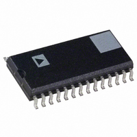
AD7719BR Analog Devices Inc, AD7719BR Datasheet - Page 23

AD7719BR
Manufacturer Part Number
AD7719BR
Description
IC ADC 16BIT 24BIT DUAL 28-SOIC
Manufacturer
Analog Devices Inc
Datasheet
1.AD7719BRUZ-REEL.pdf
(40 pages)
Specifications of AD7719BR
Number Of Bits
16/24
Sampling Rate (per Second)
105
Data Interface
DSP, MICROWIRE™, QSPI™, Serial, SPI™
Number Of Converters
2
Power Dissipation (max)
4.5mW
Voltage Supply Source
Analog and Digital
Operating Temperature
-40°C ~ 85°C
Mounting Type
Surface Mount
Package / Case
28-SOIC (0.300", 7.50mm Width)
For Use With
EVAL-AD7719EB - BOARD EVAL FOR AD7719
Lead Free Status / RoHS Status
Contains lead / RoHS non-compliant
Available stocks
Company
Part Number
Manufacturer
Quantity
Price
Part Number:
AD7719BRZ
Manufacturer:
ADI/亚德诺
Quantity:
20 000
Bit Location
AD0CON2
AD0CON1
AD0CON0
Aux ADC Control Registers (AD1CON):
(A3, A2, A1, A0 = 0, 0, 1, 1; Power-On Reset = 0x00)
The aux ADC control register is an 8-bit register from which data
can be read or to which data can be written. This register is used
to configure the aux ADC for range, channel selection, and uni-
polar or bipolar coding. Table XIV outlines the bit designations
Bit Location
AD1CON7
AD1CON6
AD1CON5
AD1CON4
CHCON
0
0
0
0
0
1
1
1
1
1
X
X
X
AD1CON3
AD1CON2
AD1CON1
AD1CON0
NOTES
1. When the temperature sensor is selected, the AD7719 automatically selects its internal reference. The temperature sensor is not factory calibrated. Temp sensor
2. A 1°C change in temperature will normally result in a 256 LSB change in the AD1 data register (ADC conversion result).
REV. A
is suitable for relative temperature measurements. The temperature sensor yields conversion results where a conversion result of 0x8000 equates to typically 0°C.
A
A
D
D
1
1
E
C
N
O
Bit Name
AD1EN
ACH2
ACH1
ACH0
ACH2
0
0
0
0
1
0
0
0
0
1
1
1
1
U/B
0
0
ARN
N
(
) 0
7
Bit Name
RN2
RN1
RN0
A
A
D
Table XIII. Main ADC Control Register (AD0CON) Bit Designations (continued)
C
1
H
C
2
O
(
Description
Aux ADC Enable Bit.
Set by user to enable the Aux ADC. When set, the aux ADC operates according to the MD bits
in the mode register.
Cleared by the user to power down the aux ADC.
Aux ADC Channel Selection Bits.
Written by the user to select the active input channels used by the aux ADC as follows:
ACH1
0
0
1
1
0
0
0
1
1
0
0
1
1
Aux ADC Unipolar/Bipolar Selection Bit.
Set by user to enable unipolar coding, i.e., zero differential input will result in 0x0000 output.
Cleared by user to enable bipolar coding, zero differential input will result in 0x8000 output.
Must be zero for specified operation.
Must be zero for specified operation.
Auxiliary Channel Input Range Bit.
When set by the user, the input range is ±REFIN2. When cleared by the user, the input range is ±REFIN2/2.
N
Table XIV. Aux ADC Control Register (AD1CON) Bit Designations
) 0
Main ADC Range Bits.
Written by the user to select the main ADC input range as follows.
Description
RN2
0
0
0
0
1
1
1
1
6
A
A
D
C
1
H
C
ACH0
0
1
0
1
0
0
1
0
1
0
1
0
1
1
RN1
0
0
1
1
0
0
1
1
O
(
N
) 0
5
A
A
D
Positive Input
AIN3
AIN4
AIN5
Temp Sensor
AGND
AIN5
AIN6
AIN5
Temp Sensor
AGND
Not Defined
Not Defined
Not Defined
C
1
H
RN0
0
1
0
1
0
1
0
1
C
0
O
(
N
) 0
4
–23–
A
for the aux ADC control register. AD1CON7 through AD1CON0
indicate the bit location, with AD1CON denoting that the bits
are in the aux ADC control register. AD1CON7 denotes the
first bit of the data stream. The number in parentheses indicates
the power-on/reset default status of that bit.
D
U B
Selected Main ADC Input Range (V
±20 mV
±40 mV
±80 mV
±160 mV
±320 mV
±640 mV
±1.28 V
±2.56 V
1
/
C
O
(
Negative Input
AGND
AGND
AIN6
(Temp Sensor Routed to the ADC Inputs)
AGND (Internal Short)
AGND
AGND
AIN6
(Temp Sensor Routed to the ADC Inputs)
AGND (Internal Short)
) 0
N
3
A
D
0
1
C
(
) 0
O
N
2
A
D
0
1
C
(
) 0
O
REF
N
1
= 2.5 V)
A
A
D
AD7719
R
1
N
C
O
(
) 1
N
0


