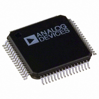
AD9238BSTRL-20 Analog Devices Inc, AD9238BSTRL-20 Datasheet - Page 10

AD9238BSTRL-20
Manufacturer Part Number
AD9238BSTRL-20
Description
IC ADC 12BIT DUAL 20MSPS 64-LQFP
Manufacturer
Analog Devices Inc
Datasheet
1.AD9238BSTZ-40.pdf
(48 pages)
Specifications of AD9238BSTRL-20
Rohs Status
RoHS non-compliant
Number Of Bits
12
Sampling Rate (per Second)
20M
Data Interface
Parallel
Number Of Converters
2
Power Dissipation (max)
180mW
Voltage Supply Source
Single Supply
Operating Temperature
-40°C ~ 85°C
Mounting Type
Surface Mount
Package / Case
64-LQFP
AD9238
TERMINOLOGY
Aperture Delay
SHA performance measured from the rising edge of the clock
input to when the input signal is held for conversion.
Aperture Jitter
The variation in aperture delay for successive samples, which is
manifested as noise on the input to the ADC.
Integral Nonlinearity (INL)
Deviation of each individual code from a line drawn from
negative full scale through positive full scale. The point used as
negative full scale occurs ½ LSB before the first code transition.
Positive full scale is defined as a level 1½ LSB beyond the last
code transition. The deviation is measured from the middle of
each particular code to the true straight line.
Differential Nonlinearity (DNL, No Missing Codes)
An ideal ADC exhibits code transitions that are exactly 1 LSB
apart. DNL is the deviation from this ideal value. Guaranteed
no missing codes to 12-bit resolution indicates that all 4,096
codes must be present over all operating ranges.
Offset Error
The major carry transition should occur for an analog value
½ LSB below VIN+ = VIN−. Offset error is defined as the
deviation of the actual transition from that point.
Gain Error
The first code transition should occur at an analog value ½ LSB
above negative full scale. The last transition should occur at an
analog value 1½ LSB below the nominal full scale. Gain error is
the deviation of the actual difference between first and last code
transitions and the ideal difference between first and last code
transitions.
Temperature Drift
The temperature drift for zero error and gain error specifies the
maximum change from the initial (25°C) value to the value at
T
Power Supply Rejection
The specification shows the maximum change in full scale from
the value with the supply at the minimum limit to the value
with the supply at its maximum limit.
Total Harmonic Distortion (THD)
The ratio of the rms sum of the first six harmonic components
to the rms value of the measured input signal, expressed as a
percentage or in decibels relative to the peak carrier signal (dBc).
Signal-to-Noise and Distortion (SINAD) Ratio
The ratio of the rms value of the measured input signal to the
rms sum of all other spectral components below the Nyquist
MIN
or T
MAX
.
Rev. C | Page 10 of 48
frequency, including harmonics but excluding dc. The value for
SINAD is expressed in dB.
Effective Number of Bits (ENOB)
Using the following formula
ENOB for a device for sine wave inputs at a given input
frequency can be calculated directly from its measured SINAD.
Signal-to-Noise Ratio (SNR)
The ratio of the rms value of the measured input signal to the
rms sum of all other spectral components below the Nyquist
frequency, excluding the first six harmonics and dc. The value
for SNR is expressed in dB.
Spurious-Free Dynamic Range (SFDR)
The difference in dB between the rms amplitude of the input
signal and the peak spurious signal, which may or may not be a
harmonic.
Nyquist Sampling
When the frequency components of the analog input are below
the Nyquist frequency (f
Nyquist sampling.
IF Sampling
Due to the effects of aliasing, an ADC is not limited to Nyquist
sampling. Higher sampled frequencies are aliased down into the
first Nyquist zone (DC − f
The bandwidth of the sampled signal should not overlap
Nyquist zones and alias onto itself. Nyquist sampling
performance is limited by the bandwidth of the input SHA and
clock jitter (jitter adds more noise at higher input frequencies).
Two-Tone SFDR
The ratio of the rms value of either input tone to the rms value
of the peak spurious component. The peak spurious component
may or may not be an IMD product.
Out-of-Range Recovery Time
The time it takes for the ADC to reacquire the analog input
after a transient from 10% above positive full scale to 10% above
negative full scale, or from 10% below negative full scale to 10%
below positive full scale.
Crosstalk
Coupling onto one channel being driven by a (−0.5 dBFS) signal
when the adjacent interfering channel is driven by a full-scale
signal. Measurement includes all spurs resulting from both
direct coupling and mixing components.
ENOB = (SINAD − 1.76)/6.02
CLOCK
CLOCK
/2), this is often referred to as
/2) on the output of the ADC.


