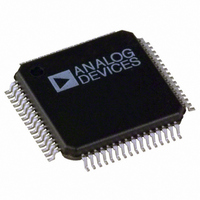
AD9238BSTRL-20 Analog Devices Inc, AD9238BSTRL-20 Datasheet - Page 16

AD9238BSTRL-20
Manufacturer Part Number
AD9238BSTRL-20
Description
IC ADC 12BIT DUAL 20MSPS 64-LQFP
Manufacturer
Analog Devices Inc
Datasheet
1.AD9238BSTZ-40.pdf
(48 pages)
Specifications of AD9238BSTRL-20
Rohs Status
RoHS non-compliant
Number Of Bits
12
Sampling Rate (per Second)
20M
Data Interface
Parallel
Number Of Converters
2
Power Dissipation (max)
180mW
Voltage Supply Source
Single Supply
Operating Temperature
-40°C ~ 85°C
Mounting Type
Surface Mount
Package / Case
64-LQFP
AD9238
THEORY OF OPERATION
The AD9238 consists of two high performance ADCs that are
based on the AD9235 converter core. The dual ADC paths are
independent, except for a shared internal band gap reference
source, VREF. Each of the ADC paths consists of a proprietary
front end SHA followed by a pipelined switched-capacitor
ADC. The pipelined ADC is divided into three sections,
consisting of a 4-bit first stage, followed by eight 1.5-bit stages,
and a final 3-bit flash. Each stage provides sufficient overlap to
correct for flash errors in the preceding stages. The quantized
outputs from each stage are combined through the digital
correction logic block into a final 12-bit result. The pipelined
architecture permits the first stage to operate on a new input
sample, while the remaining stages operate on preceding samples.
Sampling occurs on the rising edge of the respective clock.
Each stage of the pipeline, excluding the last, consists of a low
resolution flash ADC and a residual multiplier to drive the next
stage of the pipeline. The residual multiplier uses the flash ADC
output to control a switched-capacitor digital-to-analog
converter (DAC) of the same resolution. The DAC output is
subtracted from the stage’s input signal and the residual is
amplified (multiplied) to drive the next pipeline stage. The
residual multiplier stage is also called a multiplying DAC
(MDAC). One bit of redundancy is used in each one of the
stages to facilitate digital correction of flash errors. The last
stage simply consists of a flash ADC.
The input stage contains a differential SHA that can be
configured as ac- or dc-coupled in differential or single-ended
modes. The output-staging block aligns the data, carries out the
error correction, and passes the data to the output buffers. The
output buffers are powered from a separate supply, allowing
adjustment of the output voltage swing.
ANALOG INPUT
The analog input to the AD9238 is a differential, switched-
capacitor, SHA that has been designed for optimum perfor-
mance while processing a differential input signal. The SHA
input accepts inputs over a wide common-mode range. An
input common-mode voltage of midsupply is recommended to
maintain optimal performance.
The SHA input is a differential, switched-capacitor circuit. In
Figure 32, the clock signal alternatively switches the SHA
between sample mode and hold mode. When the SHA is
switched into sample mode, the signal source must be capable
of charging the sample capacitors and settling within one-half
of a clock cycle. A small resistor in series with each input can
help reduce the peak transient current required from the output
stage of the driving source. Also, a small shunt capacitor can be
placed across the inputs to provide dynamic charging currents.
This passive network creates a low-pass filter at the ADC input;
therefore, the precise values are dependent on the application.
Rev. C | Page 16 of 48
In IF undersampling applications, any shunt capacitors should
be removed. In combination with the driving source
impedance, they limit the input bandwidth. For best dynamic
performance, the source impedances driving VIN+ and VIN−
should be matched such that common-mode settling errors are
symmetrical. These errors are reduced by the common-mode
rejection of the ADC.
An internal differential reference buffer creates positive and
negative reference voltages, REFT and REFB, respectively, that
define the span of the ADC core. The output common mode of
the reference buffer is set to midsupply, and the REFT and
REFB voltages and span are defined as:
The equations above show that the REFT and REFB voltages are
symmetrical about the midsupply voltage and, by definition, the
input span is twice the value of the VREF voltage.
The internal voltage reference can be pin-strapped to fixed
values of 0.5 V or 1.0 V or adjusted within the same range as
discussed in the Internal Reference Connection section.
Maximum SNR performance is achieved with the AD9238 set
to the largest input span of 2 V p-p. The relative SNR
degradation is 3 dB when changing from 2 V p-p mode to
1 V p-p mode.
The SHA may be driven from a source that keeps the signal
peaks within the allowable range for the selected reference
voltage. The minimum and maximum common-mode input
levels are defined as:
VIN–
VIN+
REFT = ½(AVDD + VREF)
REFB = ½ (AVDD −VREF)
Span = 2 × (REFT − REFB) = 2 × VREF
VCM
VCM
C
C
PAR
PAR
MIN
MAX
= VREF/2
= (AVDD + VREF)/2
Figure 32. Switched-Capacitor Input
T
T
5pF
5pF
T
T
H
H


