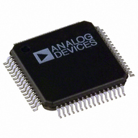
AD9238BSTRL-20 Analog Devices Inc, AD9238BSTRL-20 Datasheet - Page 34

AD9238BSTRL-20
Manufacturer Part Number
AD9238BSTRL-20
Description
IC ADC 12BIT DUAL 20MSPS 64-LQFP
Manufacturer
Analog Devices Inc
Datasheet
1.AD9238BSTZ-40.pdf
(48 pages)
Specifications of AD9238BSTRL-20
Rohs Status
RoHS non-compliant
Number Of Bits
12
Sampling Rate (per Second)
20M
Data Interface
Parallel
Number Of Converters
2
Power Dissipation (max)
180mW
Voltage Supply Source
Single Supply
Operating Temperature
-40°C ~ 85°C
Mounting Type
Surface Mount
Package / Case
64-LQFP
AD9238
DUAL ADC LFCSP PCB
The LFCSP PCB requires a low jitter clock source, analog sources,
and power supplies. The PCB interfaces directly with Analog
Devices standard dual-channel data capture board (HSC-ADC-
EVAL-DC), which together with ADI’s ADC Analyzer™ software
allows for quick ADC evaluation.
POWER CONNECTOR
Power is supplied to the board via three detachable 4-lead
power strips.
Table 11. Power Connector
Terminal
VCC
VDD
VDL
VREF
+5 V
−5 V
1
ANALOG INPUTS
The evaluation board accepts a 2 V p-p analog input signal
centered at ground at two SMB connectors, Input A and
Input B. These signals are terminated at their respective
transformer primary side. T1 and T2 are wideband RF
transformers that provide the single-ended-to-differential
conversion, allowing the ADC to be driven differentially,
minimizing even-order harmonics. The analog signals can be
low-pass filtered at the transformer secondary to reduce high
frequency aliasing.
OPTIONAL OPERATIONAL AMPLIFIER
The PCB has been designed to accommodate an optional
AD8139 op amp that can serve as a convenient solution for
dc-coupled applications. To use the AD8139 op amp, remove
C14, R4, R5, C13, R37, and R36. Place R22, R23, R30, and R24.
VCC, VDD, and VDL are the minimum required power connections.
1
1
1
3.0 V
3.0 V
3.0 V
Comments
Analog supply for ADC
Output supply for ADC
Supply circuitry
Optional external VREF
Optional op amp supply
Optional op amp supply
Rev. C | Page 34 of 48
CLOCK
The clock inputs are buffered on the board at U5 and U6. These
gates provide buffered clocks to the on-board latches, U2 and
U4, ADC input clocks, and DRA and DRB that are available at
the output Connector P3, P8. The clocks can be inverted at the
timing jumpers labeled with the respective clocks. The clock
paths also provide for various termination options. The ADC
input clocks can be set to bypass the buffers at P2 to P9 and
P10, P12. An optional clock buffer U3, U7 can also be placed.
The clock inputs can be bridged at TIEA, TIEB (R20, R40) to
allow one to clock both channels from one clock source; however,
optimal performance is obtained by driving J2 and J3.
Table 12. Jumpers
Terminal
OEB A
PDWN A
MUX
SHARED REF
DR A
LATA
ENC A
OEB B
PDWN B
DFS
SHARED REF
DR B
LATB
ENC B
VOLTAGE REFERENCE
The ADC SENSE pin is brought out to E41, and the internal
reference mode is selected by placing a jumper from E41 to
ground (E27). External reference mode is selected by placing a
jumper from E41 to E25 and E30 to E2. R56 and R45 allow for
programmable reference mode selection.
DATA OUTPUTS
The ADC outputs are latched on the PCB at U2 and U4. The
ADC outputs have the recommended series resistors in line to
limit switching transient effects on ADC performance.
Shared Reference Input
Invert A Latch Clock
Shared Reference Input
Invert B Latch Clock
Comments
Output Enable for A Side
Power-Down A
Mux Input
Invert DR A
Invert Encode A
Output Enable for B Side
Power-Down B
Data Format Select
Invert DR B
Invert Encode B


