TSA1401IF STMicroelectronics, TSA1401IF Datasheet
TSA1401IF
Specifications of TSA1401IF
Available stocks


Related parts for TSA1401IF


TSA1401IF Summary of contents
Page 1
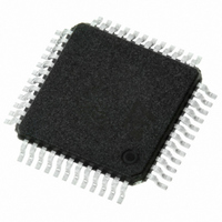
... A/D CONVERTER APPLICATIONS 1 High-end infra-red imaging X-Ray medical imaging High-end CCD cameras Scanners and digital copiers Test instrumentation Wireless communication ORDER CODES Part Number TSA1401IF TSA1401IFT EVAL1401/AB PIN CONNECTIONS (top view) low power and dynamic PACKAGE TSA1401 Temperature Package Conditioning Range -40° ...
Page 2
TSA1401 1 ABSOLUTE MAXIMUM RATINGS Symbol AVCC, DVCC, VCCBI Analog, digital, digital buffer Supply voltage VCCBE Digital buffer Supply voltage VIN, VINB, VREFP, Analog inputs VREFM, VINCM IDout Digital output current Tstg Storage temperature ESD Electrical Static Discharge - HBM: ...
Page 3
ABSOLUTE MAXIMUM RATINGS PIN DESCRIPTIONS Pin Name I/O No IPOL I 1 VREFP I/O 2 VREFM I 3 AGND 10, 48 Analog ground. VIN I 5 VINB I 7 INCM I/O 9 AVCC I 11, 12, ...
Page 4
TSA1401 2 ELECTRICAL CHARACTERISTICS AVCC = DVCC = VCCBI =VCCBE = 2.5V, Fs= 20MHz, Fin= 10MHz, VIN-VINB@ -1.0dBFS, VREFM= 0V, VREFP=1V, INCM=0.5V (external references), Tamb = 25°C (unless otherwise specified) Timing Characteristics Symbol Parameter FS Sampling Frequency DC Clock Duty ...
Page 5
ELECTRICAL CHARACTERISTICS Dynamic Characteristics Symbol Parameter 1 Spurious Free Dynamic Range Fin=10MHz, VREFP=1V SFDR 1 Signal to Noise Ratio SNR 1 Total Harmonic Distortion THD 1 Signal to Noise and Distortion SINAD Ratio 1 Effective Number of Bits ENOB 1) ...
Page 6
TSA1401 Symbol Parameter RrefO Reference output impedance External Reference Voltage Symbol Parameter VREFP Forced Top reference voltage VREFM Bottom reference voltage VINCM Forced common mode voltage RrefI Reference input impedance Vpol Analog bias voltage Power Consumption Symbol Parameter ICCA Analog ...
Page 7
ELECTRICAL CHARACTERISTICS Digital Inputs and Outputs Symbol Parameter VIL Logic "0" voltage VIH Logic "1" voltage IIL Low input current IIH High input current Digital inputs VIL Logic "0" voltage VIH Logic "1" voltage IIL Low input current IIH High ...
Page 8
TSA1401 3 DEFINITIONS OF SPECIFIED PARAMETERS 3.1 Static Parameters Static measurements are performed through the method of histograms on a 2MHz input signal, sampled at 20Msps, which is high enough to fully characterize the test frequency response. An input level ...
Page 9
TYPICAL PERFORMANCE CHARACTERISTICS 4 TYPICAL PERFORMANCE CHARACTERISTICS Fig. 1: Linearity vs. Fin, Internal References Fs=20MHz; Icca=40mA ENOB 71 SNR Fin (Mhz) Fig. 2: Distortion vs. Fin, Internal References Fs=20MHz; Icca=40mA; ...
Page 10
TSA1401 Fig. 7: SFDR vs. input amplitude (FS=2x0.86V) Fs=20Msps; Fin=5Mhz;Icca=40mA, -20 -30 -40 -50 -60 SFDR(dBc) -70 -80 -90 SFDR(dBFS) -100 -110 -30 -25 -20 -15 SFSR(dB) Fig. 8: Single-tone 16K FFT at Fs=20 Msps, Internal references Fin=5MHz, Icca=40mA,Vin@-1dBFS, SFDR=-89.3dBc, ...
Page 11
TYPICAL PERFORMANCE CHARACTERISTICS Static parameter: Differential Non Linearity Fs=20MSPS; Fin=1MHz; Icc=40mA;N=524288pts ...
Page 12
TSA1401 5 APPLICATION INFORMATION The TSA1401 is a High Speed Analog to Digital converter based on a pipeline architecture and the latest deep sub micron CMOS process to achieve the best performances in terms of linearity and power consumption. The ...
Page 13
... REFP (V) An external reference voltage device may be used for specific applications requiring even better linearity, accuracy or enhanced temperature behavior. Using the STMicroelectronics TS821, TS4041-1.2 or TS431 Voltage Reference devices leads to optimum performances when configured as shown in Figure 12 . The full scale is increased to 2.5Vpp differential and SNR and SINAD are ...
Page 14
TSA1401 sampling capacitor will draw/inject a small current transient on the input signal. One method to mask this transient current is a low-pass RC filter as shown on Figure larger capacitor value compared to the sampling capacitor ...
Page 15
APPLICATION INFORMATION 5.3 - Power consumption optimization The internal architecture of the TSA1401 enables the optimization of the power consumption according to the sampling frequency of the application. For this purpose, a resistor (value Rpol) is placed between IPOL and ...
Page 16
TSA1401 - To keep the capacitive loading as low as possible at digital outputs, short lead lengths when routing are essential to minimize currents when the output changes. To minimize this output capacitance, buffers or latches close to the output ...
Page 17
APPLICATION INFORMATION Fig. 19: TSA1401 Evaluation board schematic ...
Page 18
TSA1401 Printed circuit board - List of components ...
Page 19
... No license is granted by implication or otherwise under any patent or patent rights of STMicroelectronics. Specifications mentioned in this publication are subject to change without notice. This publication supersedes and replaces all information previously supplied ...