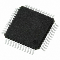
TSA1401IF STMicroelectronics, TSA1401IF Datasheet - Page 12

TSA1401IF
Manufacturer Part Number
TSA1401IF
Description
IC ADC 14BIT 20MSPS 85MW 48TQFP
Manufacturer
STMicroelectronics
Datasheet
1.TSA1401IF.pdf
(19 pages)
Specifications of TSA1401IF
Number Of Bits
14
Sampling Rate (per Second)
20M
Data Interface
Parallel
Power Dissipation (max)
85mW
Voltage Supply Source
Analog and Digital
Operating Temperature
-40°C ~ 85°C
Mounting Type
Surface Mount
Package / Case
48-TQFP, 48-VQFP
Lead Free Status / RoHS Status
Lead free / RoHS Compliant
Other names
497-4458
Available stocks
Company
Part Number
Manufacturer
Quantity
Price
Company:
Part Number:
TSA1401IF
Manufacturer:
STMicroelectronics
Quantity:
10 000
TSA1401
5 APPLICATION INFORMATION
The TSA1401 is a High Speed Analog to Digital
converter based on a pipeline architecture and the
latest deep sub micron CMOS process to achieve
the best performances in terms of linearity and
power consumption.
The pipeline structure consists of 14 internal
conversion stages in which the analog signal is
fed and sequentially converted into digital data.
Each of the 14 stages consists of an Analog to
Digital converter, a Digital to Analog converter, a
Sample and Hold and an amplifier (gain=2). A 1.5-
bit conversion resolution is achieved in each
stage. Each resulting LSB-MSB couple is then
time-shifted to recover from the delay caused by
conversion. Digital data correction completes the
processing by recovering from the redundancy of
the (LSB-MSB) couple for each stage. The
corrected data are outputted through the digital
buffers.
Signal input is sampled on the rising edge of the
clock while digital outputs are delivered on the
falling edge of the clock.
The advantages of such a converter reside in the
combination of pipeline architecture and the most
advanced technologies. The highest dynamic
performances are achieved while consumption
remains at the lowest level.
5.1 Analog Input Configuration
5.1.1 Analog input level and references
To maximize the TSA1401’s high-resolution and
speed, it is advisable to drive the analog input
differentially. The full scale of TSA1401 is
adjusted through the voltage value of VREFP and
VREFM:
VIN-VINB=2(VREFP-VREFM)
The differential analog input signal always
presents a common mode voltage, CM:
CM=(VIN+VINB)/2
In order for the user to select the right full scale
according to the application, a control pin,
REFMODE, allows to switch from internal to
external references.
12/19
Internal references, common mode:
When REFMODE is set to VIL level, TSA1401
operates with its own reference voltage generated
by its internal bandgap. VREFM pin is connected
externally to the Analog Ground while VREFP is
set to its internal voltage (0.86V). The full scale of
the ADC when using internal references is 1.8Vpp
(to reduce the full scale if desired, VREFM may be
forced externally).
In this case VREFP and INCM are low impedance
outputs. INCM pin (voltage generator 0.46V) may
be used to supply the common mode, CM of the
analog input signal.
External references, common mode:
In applications requiring a different full scale
magnitude, it is possible to force externally
VREFP and INCM (REFM must be connected to
analog ground or forced externally).
REFMODE set to VIH level will put in standby
mode the internal references. In this case,
VREFP, INCM are high impedance inputs and
have to be forced by external references.
TSA1401 shows better performances when the
full scale is increased by the use of external
references (see
Fig. 10: Linearity vs. VREFP
Fin=5MHz;Fs=20Mhz;Icca=26mA;INCM=0.45V
80
77
74
71
68
65
0.8
APPLICATION INFORMATION
0.9
Figure 10
1
REFP (V)
ENOB
SNR
1.1
and
SINAD
11
1.2
).
1.3
1.4
12.4
12.2
12
11.8
11.6
11.4
11.2
11


