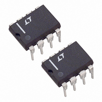
LTC1292DCN8#PBF Linear Technology, LTC1292DCN8#PBF Datasheet - Page 14

LTC1292DCN8#PBF
Manufacturer Part Number
LTC1292DCN8#PBF
Description
IC DATA ACQ SYSTEM 12BIT 8-DIP
Manufacturer
Linear Technology
Type
Data Acquisition System (DAS)r
Datasheet
1.LTC1292DCN8PBF.pdf
(24 pages)
Specifications of LTC1292DCN8#PBF
Resolution (bits)
12 b
Sampling Rate (per Second)
60k
Data Interface
Serial, Parallel
Voltage Supply Source
Single Supply
Voltage - Supply
5V
Operating Temperature
0°C ~ 70°C
Mounting Type
Through Hole
Package / Case
8-DIP (0.300", 7.62mm)
Number Of Elements
1
Resolution
12Bit
Architecture
SAR
Sample Rate
60KSPS
Input Polarity
Unipolar
Input Type
Voltage
Rated Input Volt
5V
Differential Input
Yes
Power Supply Requirement
Single
Single Supply Voltage (typ)
5V
Dual Supply Voltage (typ)
Not RequiredV
Dual Supply Voltage (min)
Not RequiredV
Dual Supply Voltage (max)
Not RequiredV
Power Dissipation
500mW
Integral Nonlinearity Error
±0.75LSB
Operating Temp Range
0C to 70C
Operating Temperature Classification
Commercial
Mounting
Through Hole
Pin Count
8
Package Type
PDIP N
Lead Free Status / RoHS Status
Lead free / RoHS Compliant
Available stocks
Company
Part Number
Manufacturer
Quantity
Price
LTC1292/LTC1297
A
Source Resistance
The analog inputs of the LTC1292/LTC1297 look like a
100pF capacitor (C
(Figures 10a and 10b). C
(–) inputs once during each conversion cycle. Large
external source resistors and capacitances will slow the
settling of the inputs. It is important that the overall RC
time constant is short enough to allow the analog inputs to
settle completely within the allowed time.
“+” Input Settling
The input capacitor for the LTC1292 is switched onto the
“+” input during the sample phase (t
11b and 11c). The sample period can be as short as t
+ 1/2 CLK cycle or as long as t
before a conversion starts. This variability depends on
where CS falls relative to CLK. The voltage on the “+” input
must settle completely within the sample period. Minimizing
R
input source resistance must be used, the sample time can
be increased by using a slower CLK frequency. With the
minimum possible sample time of 3.0 s, R
and C1 < 20pF will provide adequate settling time.
The sample period for the LTC1297 starts on the falling
edge of CS and ends on the falling edge of the first CLK
14
SOURCE
PPLICATI
+ and C1 will improve the settling time. If large “+”
(+) INPUT
(–) INPUT
D
CLK
OUT
O
CS
IN
U
) in series with a 500 resistor (R
S
IN
I FOR ATIO
gets switched between (+) and
U
WHCS
(+) INPUT MUST SETTLE DURING THIS TIME
SMPL
Figure 11a. Setup Time (t
W
+ 1 1/2 CLK cycles
, see Figures 11a,
t
WHCS
SOURCE
“+” and “–” Input Settling Windows
HI-Z
t
SMPL
U
+ < 2.0k
WHCS
ON
)
suCS
t
SUCS
(Figure 12). The length of the sample period is t
CLK cycles. Again, the voltage on the “+” input must settle
completely within the sample period. If large “+” input
source resistance must be used, the sample time can be
increased by using a slower CLK frequency or by increasing
1ST BIT TEST (–) INPUT MUST
) Is Met for the LTC1292
SETTLE DURING THIS TIME
Figure 10b. Analog Input Equivalent Circuit for the LTC1297
Figure 10a. Analog Input Equivalent Circuit for the LTC1292
V
V
V
V
IN
IN
IN
IN
+
–
+
–
R
R
R
R
SOURCE
SOURCE
SOURCE
SOURCE
+
+
–
–
B11
C1
C1
INPUT
INPUT
C2
INPUT
C2
INPUT
“–”
“+”
“–”
“+”
t
+ 0.5 CLK
B10
CS
t
+ 0.5 CLK
suCS
CS
WHCS
500
500
R
R
LTC1292/7 F11a
ON
ON
B9
LTC1297
LTC1292
C
100pF
C
100pF
LTC1292/7 F10b
LTC1292/7 F10a
IN
IN
suCS
12927fb
+0.5


