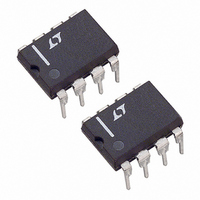
LTC1292DCN8#PBF Linear Technology, LTC1292DCN8#PBF Datasheet - Page 21

LTC1292DCN8#PBF
Manufacturer Part Number
LTC1292DCN8#PBF
Description
IC DATA ACQ SYSTEM 12BIT 8-DIP
Manufacturer
Linear Technology
Type
Data Acquisition System (DAS)r
Datasheet
1.LTC1292DCN8PBF.pdf
(24 pages)
Specifications of LTC1292DCN8#PBF
Resolution (bits)
12 b
Sampling Rate (per Second)
60k
Data Interface
Serial, Parallel
Voltage Supply Source
Single Supply
Voltage - Supply
5V
Operating Temperature
0°C ~ 70°C
Mounting Type
Through Hole
Package / Case
8-DIP (0.300", 7.62mm)
Number Of Elements
1
Resolution
12Bit
Architecture
SAR
Sample Rate
60KSPS
Input Polarity
Unipolar
Input Type
Voltage
Rated Input Volt
5V
Differential Input
Yes
Power Supply Requirement
Single
Single Supply Voltage (typ)
5V
Dual Supply Voltage (typ)
Not RequiredV
Dual Supply Voltage (min)
Not RequiredV
Dual Supply Voltage (max)
Not RequiredV
Power Dissipation
500mW
Integral Nonlinearity Error
±0.75LSB
Operating Temp Range
0C to 70C
Operating Temperature Classification
Commercial
Mounting
Through Hole
Pin Count
8
Package Type
PDIP N
Lead Free Status / RoHS Status
Lead free / RoHS Compliant
Available stocks
Company
Part Number
Manufacturer
Quantity
Price
A
If V
be turned on first, then V
met, connecting a diode from V
mended (see Figure 25).
PPLICATI
CC
Figure 23. Overvoltage Protection with Clamp Diodes
and V
V
IN
1N4148 DIODES
REF
Figure 24a. Overvoltage Protection with
Current Limiting Resistors
250
1k
O
are not tied together, then V
U
CS
+IN
–IN
GND
S
CS
+IN
–IN
GND
LTC1292
LTC1297
REF
CS
+IN
–IN
GND
TO OSCILLOSCOPE
I FOR ATIO
U
LTC1292
. If this sequence cannot be
LTC1292
LTC1297
D
V
CLK
V
OUT
REF
CC
D
22 F
V
CLK
V
OUT
REF
REF
CC
D
V
CLK
V
OUT
REF
W
CC
Figure 26. “Quick Look” Circuit for the LTC1292
LTC1292/7 F24a
to V
5V
CC
LTC1292/7 F23
is recom-
CC
5V
U
should
CLOCK IN
1MHz
f/32
Because a unique input protection structure is used on
the digital input pins, the signal levels on these pins can
exceed the device V
Figure 25. Separate V
Figure 24b. Overvoltage Protection with
Diode Clamps and Current Limiting Resistor
RESET
CLK
EN
Q1
Q2
Q3
Q4
V
1k
SS
1N4148 DIODES
CD4520
CS
+IN
–IN
GND
CC
LTC1292
LTC1297
RESET
without damaging the device.
CS
+IN
–IN
GND
LTC1292/LTC1297
V
CLK
Q4
EN
DD
Q3
Q2
Q1
LTC1292
LTC1297
D
V
CLK
V
OUT
REF
CC
CC
+5V
and V
D
V
CLK
V
OUT
REF
CC
REF
LTC1292/7 F25
1N4148
Supplies
0.1 F
LTC1292/7 F24
5V
5V
LTC1292/7 F26
5V
21
12927fb


