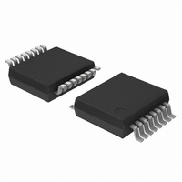
UDA1334ATS/N2,112 NXP Semiconductors, UDA1334ATS/N2,112 Datasheet - Page 7

UDA1334ATS/N2,112
Manufacturer Part Number
UDA1334ATS/N2,112
Description
IC AUDIO DAC LP 16-SSOP
Manufacturer
NXP Semiconductors
Datasheet
1.UDA1334ATSN2112.pdf
(22 pages)
Specifications of UDA1334ATS/N2,112
Number Of Converters
2
Package / Case
16-SSOP
Number Of Bits
24
Data Interface
Serial
Voltage Supply Source
Analog and Digital
Operating Temperature
-40°C ~ 85°C
Mounting Type
Surface Mount
Interface Type
Serial
Supply Voltage (max)
3.6 V
Supply Voltage (min)
2.4 V
Maximum Operating Temperature
+ 85 C
Mounting Style
SMD/SMT
Minimum Operating Temperature
- 40 C
Lead Free Status / RoHS Status
Lead free / RoHS Compliant
Power Dissipation (max)
-
Settling Time
-
Lead Free Status / Rohs Status
Lead free / RoHS Compliant
Other names
568-3443-5
935266839112
UDA1334ATSDH
935266839112
UDA1334ATSDH
NXP Semiconductors
8
8.1
The UDA1334ATS incorporates a PLL capable of
generating the system clock. The UDA1334ATS can
operate in 2 modes:
• It operates as an asynchronous DAC, which means the
• It generates the internal clocks from a 27 MHz clock
In video mode, the digital audio input is slave, which
means that the system must generate the BCK and
WS signals from the output clock available at pin CLKOUT
of the UDA1334ATS. The digital audio signals should be
frequency locked to the CLKOUT signal.
Remarks:
1. The WS edge MUST fall on the negative edge of the
2. For LSB-justified formats it is important to have a WS
8.1.1
Audio mode is enabled by setting pin PLL0 to LOW.
De-emphasis can be activated via pin DEEM/CLKOUT
according to Table 5.
In audio mode, pin SYSCLK/PLL1 is used to set the
sampling frequency range as given in Table 1.
Table 1 Sampling frequency range in audio mode
8.1.2
In video mode, the master clock is a 27 MHz external clock
(as is available in video environment). A clock-out signal is
generated at pin DEEM/CLKOUT. The output frequency
can be selected using pin PLL0. The output frequency is
either 12.228 MHz (256 × 48 kHz) with pin PLL0 being at
MID level or 18.432 MHz (384 × 48 kHz) with pin PLL0
being HIGH, as given in Table 2.
2000 Jul 31
SYSCLK/PLL1
device regenerates the internal clocks using a PLL from
the incoming WS signal. This mode is called audio
mode.
input, based on 32, 48 and 96 kHz sampling
frequencies. This mode is called video mode.
Low power audio DAC with PLL
BCK at all times for proper operation of the digital I/O
data interface
signal with a duty factor of 50%.
FUNCTIONAL DESCRIPTION
HIGH
System clock
LOW
A
V
IDEO MODE
UDIO MODE
f
f
s
s
= 16 to 50 kHz
= 50 to 100 kHz
SELECTION
7
Table 2 Clock output selection in video mode
Notes
1. The supported sampling frequencies are:
2. The supported sampling frequencies are:
8.2
The interpolation digital filter interpolates from 1f
by cascading FIR filters (see Table 3).
Table 3 Interpolation filter characteristics
8.3
The 5th-order noise shaper operates at 64f
in-band quantization noise to frequencies well above the
audio band. This noise shaping technique enables high
signal-to-noise ratios to be achieved. The noise shaper
output is converted into an analog signal using a
Filter Stream DAC (FSDAC).
Pass-band ripple
Stop band
Dynamic range
96, 48 and 24 kHz or 64, 32 and 16 kHz.
96, 48 and 24 kHz; 72 and 36 kHz or 32 kHz.
HIGH
PLL0
ITEM
LOW
Noise shaper
Interpolation filter
MID
12.228 MHz clock; note 1
18.432 MHz clock; note 2
audio mode
CONDITION
0f
0f
s
s
>0.55f
to 0.45f
to 0.45f
s
SELECTION
s
s
UDA1334ATS
Product specification
VALUE (dB)
s
. It shifts
±0.02
>114
−50
s
to 64f
s


