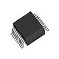
74FST3244PY IDT, Integrated Device Technology Inc, 74FST3244PY Datasheet - Page 3

74FST3244PY
Manufacturer Part Number
74FST3244PY
Description
Manufacturer
IDT, Integrated Device Technology Inc
Datasheet
1.74FST3244PY.pdf
(5 pages)
Specifications of 74FST3244PY
Logic Family
FST
Number Of Bits
8
Number Of Elements
2
Technology
CMOS
High Level Output Current
-128mA
Low Level Output Current
128mA
On Resistance
10Ohm
Propagation Delay Time
6.5ns
Package Type
SSOP
Operating Temp Range
-40C to 85C
Operating Temperature Classification
Industrial
Operating Supply Voltage (min)
4.75V
Operating Supply Voltage (typ)
5V
Operating Supply Voltage (max)
5.25V
Quiescent Current
3uA
Pin Count
20
Mounting
Surface Mount
Lead Free Status / Rohs Status
Not Compliant
Following Conditions Apply Unless Otherwise Specified:
Operating Conditions: T
NOTES:
1. See test circuit and waveforms.
2. The bus switch contributes no propagation delay other than the RC delay of the load interacting with the RC of the switch.
3. IQ
NOTES:
1. For conditions shown as Max. or Min., use appropriate value specified under Electrical Characteristics for the applicable device type.
2. Typical values are at V
3. Per TTL driven input (V
4. This parameter is not directly testable, but is derived for use in Total Power Supply Calculations.
5. C
6. I
IDT74FST3244
OCTAL BUS SWITCH
Symbol
t
t
t
t
t
t
|Q
PLH
PHL
PZH
PZL
PHZ
PLZ
C
I
I
D
N
I
f
N = Number of Switches Toggling at f
All currents are in milliamps and all frequencies are in megahertz.
IQ
from the DISCONNECT of the first path is compensated by the CONNECT of the second path.
C
C
CC
CCD
i
I
CI
PD
PD
H
T
Symbol
CC
= Input Frequency
I
I
= I
= I
DCI
CCD
C
|
CI
= Number of TTL Inputs at D
= Duty Cycle for TTL Inputs High
I
= Quiescent Current
CC
= I
I is the charge injection for a single switch DISCONNECT and applies to either single switches or multiplexers.
= Power Dissipation Capacitance
QUIESCENT
CC
= Power Supply Current for a TTL High Input (V
= Dynamic Current Caused by an Input Transition Pair (HLH or LHL)
I is the charge injection for a multiplexer as the multiplexed port switches from one path to another. Charge Injection is reduced becasue the injection
CCD
+ I
Data Propagation Delay
A to B, B to A
Switch CONNECT Delay
x
Switch DISCONNECT Delay
x
Charge Injection During Switch DISCONNECT,
x
/V
CC
CC
to A or B
to A or B
to A or B
+ I
Quiescent Power Supply Current
TTL Inputs HIGH
Dynamic Power Supply Current
Total Power Supply Current
D
H
INPUTS
N
T
+ I
(2)
(3)
CC
A
IN
CCD
+ I
= -40°C to +85°C, V
= 5.0V, +25°C ambient.
= 3.4V). All other inputs at V
DYNAMIC
Parameter
(f
i
N)
Description
H
i
(6)
(4)
CC
= 5.0V ±5%
IN
CC
V
V
V
Outputs Open
1 Enable Pin Toggling
50% Duty Cycle
V
Outputs Open
2 Enable Pins Toggling
fi = 10MHz
50% Duty Cycle
= 3.4V)
CC
IN
CC
CC
or GND.
= 3.4V
= Max.
= Max.
= Max.
(3)
3
Test Conditions
Min.
1.5
1.5
—
—
(2)
V
V
V
V
V
V
IN
IN
IN
IN
IN
IN
= V
= GND
= V
= GND
= 3.4
= GND
(1)
CC
CC
Typ.
INDUSTRIAL TEMPERATURE RANGE
1.5
—
—
—
Min.
—
—
—
—
Typ.
120
0.5
2.4
2.9
(2)
Max.
0.25
6.5
5.5
—
Max.
160
1.5
3.2
4.7
Enable
MHz/
Unit
Unit
µ A/
mA
mA
pC
ns
ns
ns


