AD7568BP Analog Devices Inc, AD7568BP Datasheet
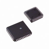
IC DAC 12BIT LC2MOS OCTAL 44PLCC

AD7568BP

Manufacturer Part Number
AD7568BP
Description
IC DAC 12BIT LC2MOS OCTAL 44PLCC
Manufacturer
Analog Devices Inc
Datasheet

Specifications of AD7568BP

Mounting Type
Surface Mount
Rohs Status
RoHS non-compliant
Settling Time
500ns
Number Of Bits
12
Data Interface
Serial
Number Of Converters
8
Voltage Supply Source
Single Supply
Power Dissipation (max)
17.5mW
Operating Temperature
-40°C ~ 85°C
Package / Case
44-PLCC
Resolution (bits)
12bit
No. Of Pins
44
Peak Reflow Compatible (260 C)
No
Update Rate
2MSPS
No. Of Bits
12 Bit
Leaded Process Compatible
No
No. Of Outputs
8
Resolution
12-Bit
Lead Free Status / RoHS Status
Contains lead / RoHS non-compliant

Available stocks

Company
Part Number
Manufacturer
Quantity
Price
Part Number:
AD7568BP
Manufacturer:
Analog Devices Inc
Quantity:
10 000
Part Number:
AD7568BPZ
Manufacturer:
Analog Devices Inc
Quantity:
135
Part Number:
AD7568BPZ
Manufacturer:
Analog Devices Inc
Quantity:
10 000
Part Number:
AD7568BPZ
Manufacturer:
ADI/亚德诺
Quantity:
20 000
Part Number:
AD7568BPZ-REEL
Manufacturer:
Analog Devices Inc
Quantity:
10 000
a
GENERAL DESCRIPTION
The AD7568 contains eight 12-bit DACs in one monolithic de-
vice. The DACs are standard current output with separate V
I
The AD7568 is a serial input device. Data is loaded using
FSIN, CLKIN and SDIN. One address pin, A0, sets up a de-
vice address, and this feature may be used to simplify device
loading in a multi-DAC environment.
All DACs can be simultaneously updated using the asynchro-
nous LDAC input and they can be cleared by asserting the
asynchronous CLR input.
The AD7568 is housed in a space-saving 44-pin plastic quad
flatpack and 44-lead PLCC.
REV. B
Information furnished by Analog Devices is believed to be accurate and
reliable. However, no responsibility is assumed by Analog Devices for its
use, nor for any infringements of patents or other rights of third parties
which may result from its use. No license is granted by implication or
otherwise under any patent or patent rights of Analog Devices.
OUT1
FEATURES
Eight 12-Bit DACs in One Package
4-Quadrant Multiplication
Separate References
Single +5 V Supply
Low Power: 1 mW
Versatile Serial Interface
Simultaneous Update Capability
Reset Function
44-Pin PQFP and PLCC
APPLICATIONS
Process Control
Automatic Test Equipment
General Purpose Instrumentation
, I
OUT2
I
I
I
I
V
OUT2
V
R
OUT1
R
V
OUT1
OUT2
R
REF
REF
REF
FB
FB
FB
NC
G
G
H
H
G
G
F
F
F
F
and R
10
11
1
2
3
4
5
6
7
8
9
FB
Plastic Quad Flatpack
terminals.
PIN 1 IDENTIFIER
AD7568 PQFP
NC = NO CONNECT
Not to Scale
(Not to Scale)
TOP VIEW
AD7568
TOP VIEW
33
32
31
30
29
28
27
26
25
24
23
NC
V
R
I
I
V
R
I
I
V
R
OUT2
OUT2
OUT1
OUT1
REF
REF
REF
FB
FB
FB
PIN CONFIGURATIONS
C
B
A
C
A
B
C
B
C
B
REF
,
One Technology Way, P.O. Box 9106, Norwood, MA 02062-9106, U.S.A.
Tel: 617/329-4700
CLKIN
SDIN
FSIN
I
I
I
I
V
V
AD7568
V
OUT1
OUT2
OUT1
OUT2
R
R
R
REF
REF
REF
FB
FB
FB
NC
A0
G
G
G
G
H
H
CONTROL LOGIC
F
F
F
F
FUNCTIONAL BLOCK DIAGRAM
INPUT SHIFT
10
11
12
13
14
15
16
17
REGISTER
7
8
9
V
DD
+
Plastic Leaded Chip Carrier
LATCH A
LATCH B
LATCH C
LATCH D
LATCH E
LATCH G
LATCH F
LATCH H
18
6
INPUT
INPUT
INPUT
INPUT
INPUT
INPUT
INPUT
INPUT
SDOUT
AGND
19
5
20
12
4
DGND
21
12
12
12
12
12
12
12
12
3
AD7568 PLCC
NC = NO CONNECT
(Not to Scale)
LDAC
22
TOP VIEW
2
LATCH
V
LATCH
LATCH
LATCH
LATCH
LATCH
LATCH
DAC A
DAC B
DAC C
DAC D
DAC E
DAC F
DAC G
LATCH
DAC H
Octal 12-Bit DAC
REF
23
1
D
CLR
44
24
V
REF
43
25
V
REF
C
12
12
12
12
12
12
12
12
42
26
V
E
REF
41
27
V
REF
B
AD7568
40
28
V
F
DAC D
DAC E
REF
DAC A
DAC B
DAC C
DAC F
DAC G
DAC H
V
Fax: 617/326-8703
REF
A
LC
39
38
37
36
35
34
33
32
31
30
29
G
R
NC
V
I
I
V
R
I
I
V
R
R
OUT1
OUT2
OUT1
OUT2
FB
V
REF
REF
FB
REF
FB
FB
REF
A
2
C
B
A
C
B
A
C
C
B
B
H
MOS
I
I
I
R
I
I
R
I
I
I
R
I
I
I
I
R
I
I
R
R
I
I
R
OUT1
OUT2
OUT2
OUT2
OUT2
OUT1
OUT1
OUT1
OUT1
OUT2
OUT1
OUT2
OUT1
OUT2
OUT1
OUT2
FB
FB
FB
FB
FB
FB
FB
B
C
E
H
D
F
G
A
A
C
B
B
C
D
D
E
E
F
F
G
G
H
H

Related parts for AD7568BP

AD7568BP Summary of contents

Page 1

FEATURES Eight 12-Bit DACs in One Package 4-Quadrant Multiplication Separate References Single +5 V Supply Low Power Versatile Serial Interface Simultaneous Update Capability Reset Function 44-Pin PQFP and PLCC APPLICATIONS Process Control Automatic Test Equipment General Purpose ...

Page 2

AD7568–SPECIFICATIONS Parameter AD7568B ACCURACY Resolution 12 Relative Accuracy Differential Nonlinearity Gain Error + MIN MAX Gain Temperature Coefficient 2 5 Output Leakage Current I OUT1 @ + 200 MIN MAX REFERENCE ...

Page 3

... DB15 DB0 t 8 DB15 t 9 Figure 1. Timing Diagram +2.1V Model AD7568BS AD7568BP *S = Plastic Quad Flatpack (PQFP Plastic Leaded Chip Carrier (PLCC). –3– AD7568 unless otherwise noted) MIN MAX Description CLKIN Cycle Time CLKIN High Time CLKIN Low Time FSIN Setup Time ...

Page 4

AD7568 1 ABSOLUTE MAXIMUM RATINGS (T = +25 C unless otherwise noted DGND . . . . . . . . . . . . . . . . . . . . . . . . ...

Page 5

TERMINOLOGY Relative Accuracy Relative Accuracy or endpoint linearity is a measure of the maximum deviation from a straight line passing through the endpoints of the DAC transfer function measured after adjusting for zero error and full-scale error and ...

Page 6

AD7568 –Typical Performance Curves 5 +25 C 4.5 A 4.0 3.5 3.0 2.5 2.0 1.5 1.0 0.5 0.0 0.0 1.0 2.0 3.0 4.0 5.0 DIGITAL INPUT – Volts Figure 3. Supply Current vs. ...

Page 7

DAC LOADED WITH ALL 1s –10 – + +25 C – 20V pk-pk IN –40 OP AMP = AD713 –50 –60 –70 DAC LOADED WITH ALL 0s –80 –90 –100 3 ...

Page 8

AD7568 UNIPOLAR BINARY OPERATION (2-Quadrant Multiplication) Figure 15 shows the standard unipolar binary connection dia- gram for one of the DACs in the AD7568. When V signal, the circuit performs 2-quadrant multiplication. Resistors R1 and R2 allow the user to ...

Page 9

Current Mode Circuit In the current mode circuit of Figure 17 biased positive by an amount V OUT1 operate correctly, the DAC ladder termination resistor must be connected internally This is the case ...

Page 10

AD7568 In the circuit of Figure (i.e., the same code is loaded to each DAC). Resonant frequency 1/(2 R3C1). 0 Quality Factor (R6/R8)•(R2/R5). Bandpass Gain, A0 ...

Page 11

PC5 PC6 PC7 SCK MOSI *ADDITIONAL PINS OMITTED FOR CLARITY Figure 21. AD7568 to 68HC11 Interface In Figure 21, LDAC and CLR are controlled by the PC6 and PC5 port outputs. As with the 80C51, each DAC of the ...

Page 12

AD7568 For systems which contain larger numbers of AD7568s and where the user also wishes to read back the DAC contents for diagnostic purposes, the SDOUT pin may be used to daisy chain several devices together and provide the necessary ...

Related keywords