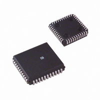
AD7568BP Analog Devices Inc, AD7568BP Datasheet - Page 10

AD7568BP
Manufacturer Part Number
AD7568BP
Description
IC DAC 12BIT LC2MOS OCTAL 44PLCC
Manufacturer
Analog Devices Inc
Datasheet
1.AD7568BPZ-REEL.pdf
(12 pages)
Specifications of AD7568BP
Mounting Type
Surface Mount
Rohs Status
RoHS non-compliant
Settling Time
500ns
Number Of Bits
12
Data Interface
Serial
Number Of Converters
8
Voltage Supply Source
Single Supply
Power Dissipation (max)
17.5mW
Operating Temperature
-40°C ~ 85°C
Package / Case
44-PLCC
Resolution (bits)
12bit
No. Of Pins
44
Peak Reflow Compatible (260 C)
No
Update Rate
2MSPS
No. Of Bits
12 Bit
Leaded Process Compatible
No
No. Of Outputs
8
Resolution
12-Bit
Lead Free Status / RoHS Status
Contains lead / RoHS non-compliant
Available stocks
Company
Part Number
Manufacturer
Quantity
Price
Company:
Part Number:
AD7568BPZ
Manufacturer:
Analog Devices Inc
Quantity:
135
Company:
Part Number:
AD7568BPZ
Manufacturer:
Analog Devices Inc
Quantity:
10 000
Part Number:
AD7568BPZ
Manufacturer:
ADI/亚德诺
Quantity:
20 000
Company:
Part Number:
AD7568BPZ-REEL
Manufacturer:
Analog Devices Inc
Quantity:
10 000
AD7568
In the circuit of Figure 19:
Using the values shown in Figure 19, the Q range is 0.3 to 5,
and the f
APPLICATION HINTS
Output Offset
CMOS D/A converters in circuits such as Figures 15, 16 and 17
exhibit a code dependent output resistance which in turn can
cause a code dependent error voltage at the output of the ampli-
fier. The maximum amplitude of this error, which adds to the
D/A converter nonlinearity, depends on V
amplifier input offset voltage. For the AD7568 to maintain
specified accuracy with V
V
temperature range of operation. Suitable amplifiers include the
AD OP07, AD OP27, OP177, AD711, AD845 or multiple ver-
sions of these.
Temperature Coefficients
The gain temperature coefficient of the AD7568 has a maxi-
mum value of 5 ppm/ C and a typical value of 2 ppm/ C. This
corresponds to gain shifts of 2 LSBs and 0.8 LSBs respectively
over a 100 C temperature range. When trim resistors R1 and
R2 are used to adjust full-scale in Figures 15 and 16, their tem-
perature coefficients should be taken into account. For further
information see “Gain Error and Gain Temperature Coefficient
of CMOS Multiplying DACs,” Application Note, Publication
Number E630c–5–3/86, available from Analog Devices.
High Frequency Considerations
The output capacitances of the AD7568 DACs work in con-
junction with the amplifier feedback resistance to add a pole to
the open loop response. This can cause ringing or oscillation.
Stability can be restored by adding a phase compensation ca-
pacitor in parallel with the feedback resistor. This is shown as
C1 in Figures 15, 16 and 17.
MICROPROCESSOR INTERFACING
AD7568–80C51 Interface
A serial interface between the AD7568 and the 80C51 micro-
controller is shown in Figure 20. TXD of the 80C51 drives
SCLK of the AD7568 while RXD drives the serial data line of
the part. The FSIN signal is derived from the port line P3.3.
The 80C51 provides the LSB of its SBUF register as the first bit
in the serial data stream. Therefore, the user will have to ensure
that the data in the SBUF register is arranged correctly so that
OS
C1 = C2, R7 = R8, R3 = R4 (i.e., the same code is loaded to
each DAC).
Resonant frequency, f
Quality Factor, Q = (R6/R8)•(R2/R5).
Bandpass Gain, A0 = –R2/R1.
be no greater than 500 V, or (50
0
range is 0 to 12 kHz.
0
REF
= 1/(2 R3C1).
at 10 V, it is recommended that
10
OS
–6
, where V
)•(V
REF
), over the
OS
is the
–10–
the data word transmitted to the AD7568 corresponds to the
loading sequence shown in Table I. When data is to be trans-
mitted to the part, P3.3 is taken low. Data on RXD is valid on
the falling edge of TXD. The 80C51 transmits its serial data in
8-bit bytes with only eight falling clock edges occurring in the
transmit cycle. To load data to the AD7568, P3.3 is left low af-
ter the first eight bits are transferred, and a second byte of data
is then transferred serially to the AD7568. When the second se-
rial transfer is complete, the P3.3 line is taken high. Note that
the 80C51 outputs the serial data byte in a format which has the
LSB first. The AD7568 expects the MSB first. The 80C51
transmit routine should take this into account.
LDAC and CLR on the AD7568 are also controlled by 80C51
port outputs. The user can bring LDAC low after every two
bytes have been transmitted to update the DAC which has been
programmed. Alternatively, it is possible to wait until all the in-
put registers have been loaded (sixteen byte transmits) and then
update the DAC outputs.
AD7568–68HC11 Interface
Figure 21 shows a serial interface between the AD7568 and the
68HC11 microcontroller. SCK of the 68HC11 drives SCLK of
the AD7568, while the MOSI output drives the serial data line
of the AD7568. The FSIN signal is derived from a port line
(PC7 shown).
For correct operation of this interface, the 68HC11 should be
configured such that its CPOL bit is a 0 and its CPHA bit is a 1.
When data is to be transmitted to the part, PC7 is taken low.
When the 68HC11 is configured like this, data on MOSI is valid
on the falling edge of SCK. The 68HC11 transmits its serial
data in 8-bit bytes (MSB first), with only eight falling clock
edges occurring in the transmit cycle. To load data to the
AD7568, PC7 is left low after the first eight bits are transferred,
and a second byte of data is then transferred serially to the
AD7568. When the second serial transfer is complete, the PC7
line is taken high.
Figure 20. AD7568 to 80C51 Interface
*ADDITIONAL PINS OMITTED FOR CLARITY
80C51*
P3.5
P3.4
P3.3
RXD
TXD
CLR
LDAC
FSIN
SCLK
SDIN
AD7568*
REV. B


