AD7568BP Analog Devices Inc, AD7568BP Datasheet - Page 4
AD7568BP
Manufacturer Part Number
AD7568BP
Description
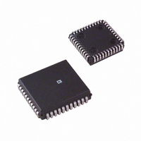
IC DAC 12BIT LC2MOS OCTAL 44PLCC
Manufacturer
Analog Devices Inc
Datasheet
1.AD7568BPZ-REEL.pdf
(12 pages)
Specifications of AD7568BP
Mounting Type
Surface Mount
Rohs Status
RoHS non-compliant
Settling Time
500ns
Number Of Bits
12
Data Interface
Serial
Number Of Converters
8
Voltage Supply Source
Single Supply
Power Dissipation (max)
17.5mW
Operating Temperature
-40°C ~ 85°C
Package / Case
44-PLCC
Resolution (bits)
12bit
No. Of Pins
44
Peak Reflow Compatible (260 C)
No
Update Rate
2MSPS
No. Of Bits
12 Bit
Leaded Process Compatible
No
No. Of Outputs
8
Resolution
12-Bit
Lead Free Status / RoHS Status
Contains lead / RoHS non-compliant
Available stocks
Company
Part Number
Manufacturer
Quantity
Price

Company:
Part Number:
AD7568BPZ
Manufacturer:
Analog Devices Inc
Quantity:
135
Company:
Part Number:
AD7568BPZ
Manufacturer:
Analog Devices Inc
Quantity:
10 000
Part Number:
AD7568BPZ
Manufacturer:
ADI/亚德诺
Quantity:
20 000
Company:
Part Number:
AD7568BPZ-REEL
Manufacturer:
Analog Devices Inc
Quantity:
10 000


AD7568
ABSOLUTE MAXIMUM RATINGS
(T
V
I
I
Digital Input Voltage to DGND . . . . . . –0.3 V to V
V
Input Current to Any Pin Except Supplies
Operating Temperature Range
CAUTION
ESD (electrostatic discharge) sensitive device. Electrostatic charges as high as 4000 V readily
accumulate on the human body and test equipment and can discharge without detection.
Although the AD7568 features proprietary ESD protection circuitry, permanent damage may
occur on devices subjected to high energy electrostatic discharges. Therefore, proper ESD
precautions are recommended to avoid performance degradation or loss of functionality.
Pin
V
DGND
AGND
V
R
I
AGND
CLKIN
FSIN
SDIN
SDOUT
A0
LDAC
CLR
OUT1
OUT2
OUT
DD
RFB
A
DD
REF
FB
Commercial Plastic (B Versions) . . . . . . . . –40 C to +85 C
= +25 C unless otherwise noted)
A – R
to DGND . . . . . . . . . . . . . . . . . . . . . . . . . –0.3 V to +6 V
, V
A – I
A – V
to DGND . . . . . . . . . . . . . . . . . . . –0.3 V to V
to DGND . . . . . . . . . . . . . . . . . . . –0.3 V to V
REF
FB
OUT
REF
to DGND . . . . . . . . . . . . . . . . . . . . . . . . . . 15 V
H
H
H
Description
Positive power supply. This is +5 V
Digital Ground.
Analog Ground.
DAC reference inputs.
DAC feedback resistor pins.
DAC current output terminals.
This pin connects to the back gates of the current steering switches. It should be connected to the signal ground
of the system.
Clock Input. Data is clocked into the input shift register on the falling edges of CLKIN.
Level-triggered control input (active low). This is the frame synchronization signal for the input data. When
FSIN goes low, it enables the input shift register, and data is transferred on the falling edges of CLKIN. If the
address bit is valid, the 12-bit DAC data is transferred to the appropriate input latch on the sixteenth falling
edge after FSIN goes low.
Serial data input. The device accepts a 16-bit word. The first bit (DB15) is the DAC MSB, with the remaining
bits following. Next comes the device address bit, A0. If this does not correspond to the logic level on pin A0,
the data is ignored. Finally come the three DAC select bits. These determine which DAC in the device is se-
lected for loading.
This shift register output allows multiple devices to be connected in a daisy chain configuration.
Device address pin. This input gives the device an address. If DB3 of the serial input stream does not corre-
spond to this, the data which follows is ignored and not loaded to any input latch. However it will appear at
SDOUT irrespective of this.
Asynchronous LDAC input. When this input is taken low, all DAC latches are simultaneously updated with the
contents of the input latches.
Asynchronous CLR input. When this input is taken low, all DAC latch outputs go to zero.
1
2
. . . . . . . .
DD
DD
DD
PIN DESCRIPTION
+0.3 V
+0.3 V
+0.3 V
10 mA
5%.
–4–
Storage Temperature Range . . . . . . . . . . . . –65 C to +150 C
Lead Temperature (Soldering, 10 secs) . . . . . . . . . . . +300 C
Power Dissipation (Any Package) to +75 C . . . . . . . . 250 mW
Derates above +75 C by . . . . . . . . . . . . . . . . . . . . 10 mW/ C
NOTES
1
2
Stresses above those listed under “Absolute Maximum Ratings” may cause
permanent damage to the device. This is a stress rating only and functional
operation of the device at these or any other conditions above those listed in the
operational sections of this specification is not implied. Exposure to absolute
maximum rating conditions for extended periods may affect device reliability.
Transient currents of up to 100 mA will not cause SCR latch-up.
WARNING!
ESD SENSITIVE DEVICE
REV. B
Related parts for AD7568BP
Image
Part Number
Description
Manufacturer
Datasheet
Request
R

Part Number:
Description:
±1.7g Dual-Axis IMEMS Accelerometer Evaluation Board
Manufacturer:
Analog Devices Inc
Datasheet:

Part Number:
Description:
Inertial Sensor Evaluation System
Manufacturer:
Analog Devices Inc
Datasheet:
Part Number:
Description:
Manufacturer:
Analog Devices Inc
Datasheet:
Part Number:
Description:
Manufacturer:
Analog Devices Inc
Datasheet:
Part Number:
Description:
Manufacturer:
Analog Devices Inc
Datasheet:
Part Number:
Description:
Manufacturer:
Analog Devices Inc
Datasheet:
Part Number:
Description:
Manufacturer:
Analog Devices Inc
Datasheet:
Part Number:
Description:
Manufacturer:
Analog Devices Inc
Datasheet:
Part Number:
Description:
Manufacturer:
Analog Devices Inc
Datasheet:
Part Number:
Description:
Manufacturer:
Analog Devices Inc
Datasheet:
Part Number:
Description:
Manufacturer:
Analog Devices Inc
Datasheet:
Part Number:
Description:
Manufacturer:
Analog Devices Inc
Datasheet:
Part Number:
Description:
Manufacturer:
Analog Devices Inc
Datasheet: