AD7568BP Analog Devices Inc, AD7568BP Datasheet - Page 8
AD7568BP
Manufacturer Part Number
AD7568BP
Description
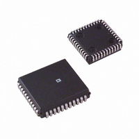
IC DAC 12BIT LC2MOS OCTAL 44PLCC
Manufacturer
Analog Devices Inc
Datasheet
1.AD7568BPZ-REEL.pdf
(12 pages)
Specifications of AD7568BP
Mounting Type
Surface Mount
Rohs Status
RoHS non-compliant
Settling Time
500ns
Number Of Bits
12
Data Interface
Serial
Number Of Converters
8
Voltage Supply Source
Single Supply
Power Dissipation (max)
17.5mW
Operating Temperature
-40°C ~ 85°C
Package / Case
44-PLCC
Resolution (bits)
12bit
No. Of Pins
44
Peak Reflow Compatible (260 C)
No
Update Rate
2MSPS
No. Of Bits
12 Bit
Leaded Process Compatible
No
No. Of Outputs
8
Resolution
12-Bit
Lead Free Status / RoHS Status
Contains lead / RoHS non-compliant
Available stocks
Company
Part Number
Manufacturer
Quantity
Price

Company:
Part Number:
AD7568BPZ
Manufacturer:
Analog Devices Inc
Quantity:
135
Company:
Part Number:
AD7568BPZ
Manufacturer:
Analog Devices Inc
Quantity:
10 000
Part Number:
AD7568BPZ
Manufacturer:
ADI/亚德诺
Quantity:
20 000
Company:
Part Number:
AD7568BPZ-REEL
Manufacturer:
Analog Devices Inc
Quantity:
10 000


AD7568
UNIPOLAR BINARY OPERATION
(2-Quadrant Multiplication)
Figure 15 shows the standard unipolar binary connection dia-
gram for one of the DACs in the AD7568. When V
signal, the circuit performs 2-quadrant multiplication. Resistors
R1 and R2 allow the user to adjust the DAC gain error. Offset
can be removed by adjusting the output amplifier offset voltage.
A1 should be chosen to suit the application. For example, the
AD OP07 or OP177 are ideal for very low bandwidth applica-
tions while the AD843 and AD845 offer very fast settling time
in wide bandwidth applications. Appropriate multiple versions
of these amplifiers can be used with the AD7568 to reduce
board space requirements.
The code table for Figure 15 is shown in Table III.
BIPOLAR OPERATION
(4-Quadrant Multiplication)
Figure 16 shows the standard connection diagram for bipolar
operation of any one of the DACs in the AD7568. The coding is
offset binary as shown in Table IV. When V
the circuit performs 4-quadrant multiplication. To maintain the
gain error specifications, resistors R3, R4 and R5 should be ra-
tio matched to 0.01%.
Digital Input
MSB………LSB
1111 1111 1111
1000 0000 0001
1000 0000 0000
0111 1111 1111
0000 0000 0001
0000 0000 0000
NOTE
Nominal LSB size for the circuit of Figure 15 is given by:
V
REF
V
(1/4096).
IN
NOTES
1. ONLY ONE DAC IS SHOWN FOR CLARITY.
2. DIGITAL INPUT CONNECTIONS ARE OMITTED.
3. C1 PHASE COMPENSATION (5–15pF) MAY BE
R1 20
Figure 15. Unipolar Binary Operation
Table III. Unipolar Binary Code Table
V
REQUIRED WHEN USING HIGH SPEED AMPLIFIER, A1.
REF
A
DAC A
AD7568
R
FB
A
Analog Output
(V
–V
–V
–V
–V
–V
–V
OUT
REF
REF
REF
REF
REF
REF
R2 10
I
I
(4095/4096)
(2049/4096)
(2048/4096)
(2047/4096)
(1/4096)
(0/4096) = 0
OUT2
OUT1
SIGNAL
As Shown in Figure 15)
GND
A
A
C1
IN
A1: OP-177
A1
is an ac signal,
ADOP-07
AD711
AD843
AD845
IN
V
OUT
is an ac
–8–
SINGLE SUPPLY CIRCUITS
The AD7568 operates from a single +5 V supply, and this
makes it ideal for single supply systems. When operating in such
a system, it is not possible to use the standard circuits of Figures
15 and 16 since these invert the analog input, V
two alternatives. One of these continues to operate the DAC as
a current-mode device, while the other uses the voltage switch-
ing mode.
Figure 16. Bipolar Operation (4-Quadrant Multiplication)
V
IN
Digital Input
MSB . . . . . LSB
1111 1111 1111
1000 0000 0001
1000 0000 0000
0111 1111 1111
0000 0000 0001
0000 0000 0000
NOTE
Nominal LSB size for the circuit of Figure 16 is given by:
V
Figure 17. Single Supply Current-Mode Operation
REF
R1 20
V
Table IV. Bipolar (Offset Binary) Code Table
(1/2048).
REF
NOTES
1. ONLY ONE DAC IS SHOWN FOR CLARITY.
2. DIGITAL INPUT CONNECTIONS ARE OMITTED.
3. C1 PHASE COMPENSATION (5–15pF) MAY BE
V
NOTES
1. ONLY ONE DAC IS SHOWN FOR CLARITY.
2. DIGITAL INPUT CONNECTIONS ARE OMITTED.
3. C1 PHASE COMPENSATION (5–15pF) MAY BE
REF
V
A
REQUIRED WHEN USING HIGH SPEED AMPLIFIER, A1.
IN
REQUIRED WHEN USING HIGH SPEED AMPLIFIER, A1.
A
AD7568
DAC A
R
FB
A
DAC A
AD7568
R
R2 10
FB
V
I
I
BIAS
OUT2
OUT1
SIGNAL
A
Analog Output
(V
+V
+V
+V
–V
–V
–V
GND
A
A
OUT
REF
REF
REF
REF
REF
REF
I
I
OUT1
OUT2
(2048/2048) = –V
(1/2048)
(2047/2048)
(2047/2048)
(1/2048)
(0/2048) = 0
As Shown in Figure 16)
C1
A
A
A1
20k
R4
A1
10k
R3
IN
V
OUT
. There are
A2
REF
20k
R5
REV. B
V
OUT
Related parts for AD7568BP
Image
Part Number
Description
Manufacturer
Datasheet
Request
R

Part Number:
Description:
±1.7g Dual-Axis IMEMS Accelerometer Evaluation Board
Manufacturer:
Analog Devices Inc
Datasheet:

Part Number:
Description:
Inertial Sensor Evaluation System
Manufacturer:
Analog Devices Inc
Datasheet:
Part Number:
Description:
Manufacturer:
Analog Devices Inc
Datasheet:
Part Number:
Description:
Manufacturer:
Analog Devices Inc
Datasheet:
Part Number:
Description:
Manufacturer:
Analog Devices Inc
Datasheet:
Part Number:
Description:
Manufacturer:
Analog Devices Inc
Datasheet:
Part Number:
Description:
Manufacturer:
Analog Devices Inc
Datasheet:
Part Number:
Description:
Manufacturer:
Analog Devices Inc
Datasheet:
Part Number:
Description:
Manufacturer:
Analog Devices Inc
Datasheet:
Part Number:
Description:
Manufacturer:
Analog Devices Inc
Datasheet:
Part Number:
Description:
Manufacturer:
Analog Devices Inc
Datasheet:
Part Number:
Description:
Manufacturer:
Analog Devices Inc
Datasheet:
Part Number:
Description:
Manufacturer:
Analog Devices Inc
Datasheet: