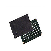
MT45W256KW16PEGA-70 WT Micron Technology Inc, MT45W256KW16PEGA-70 WT Datasheet - Page 15

MT45W256KW16PEGA-70 WT
Manufacturer Part Number
MT45W256KW16PEGA-70 WT
Description
Manufacturer
Micron Technology Inc
Datasheet
1.MT45W256KW16PEGA-70_WT.pdf
(28 pages)
Specifications of MT45W256KW16PEGA-70 WT
Operating Temperature (max)
85C
Mounting
Surface Mount
Operating Temperature Classification
Commercial
Lead Free Status / Rohs Status
Compliant
Software Access to the Configuration Register
Figure 11:
PDF: 09005aef8329b746 / Source: 09005aef82f264aa
8mb_4mb_asyncpage_cr1_0_p22z__2.fm - Rev. B 4/08 EN
Load Configuration Register
Notes:
The contents of the CR either can be read or modified using a software sequence. The
nature of this access mechanism may eliminate the need for the ZZ# ball.
If the software mechanism is used, ZZ# can simply be tied to V
cally used for ZZ# control purposes will no longer be required. However, ZZ# should not
be tied to V
software-access sequence.
The CR is loaded using a four-step sequence consisting of two READ operations followed
by two WRITE operations (see Figure 11 on page 15). The read sequence is virtually iden-
tical except that an asynchronous READ is performed during the fourth operation (see
Figure 12 on page 16).
The address used during all READ and WRITE operations is the highest address of the
CellularRAM device being accessed (3FFFFh for 4Mb); the content of this address is not
changed by using this sequence. The data bus is used to transfer data into or out of bits
15–0 of the CR.
Writing to the CR using the software sequence modifies the function of the ZZ# ball.
After the software sequence loads the CR, the level of the ZZ# ball no longer enables PAR
operation. PAR operation will be updated whenever the software sequence loads a new
value into the CR. This ZZ# functionality will continue until the next time the device is
powered up. The operation of the ZZ# ball is not affected if the software sequence is only
used to read the contents of the CR. The use of the software sequence does not affect the
ability to perform the standard (ZZ#-controlled) method of loading the CR.
LB#/UB#
1. It is possible that the data stored at the highest memory location will be altered if the data
Address
at the falling edge of WE# is not 0000h.
Data
WE#
OE#
CE#
CC
Address
(MAX)
XXXXh
Q if the system will use DPD; DPD cannot be enabled or disabled using the
READ
4Mb: 256K x16 Async/Page CellularRAM 1.0 Memory
Address
(MAX)
XXXXh
READ
15
Micron Technology, Inc., reserves the right to change products or specifications without notice.
CR: 0000h
Address
WRITE
(MAX)
0ns (MIN) see Note 1
Configuration Register Operation
WRITE
Address
CR value
(MAX)
Don’t Care
in
©2008 Micron Technology, Inc. All rights reserved.
CC
Q. The port line typi-


