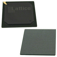
LFE3-150EA-8FN1156C Lattice, LFE3-150EA-8FN1156C Datasheet - Page 13

LFE3-150EA-8FN1156C
Manufacturer Part Number
LFE3-150EA-8FN1156C
Description
IC FPGA 149K LUTS 586I/O FN1156
Manufacturer
Lattice
Series
ECP3r
Datasheets
1.LFE3-150EA-7FN672C.pdf
(136 pages)
2.LFE3-35EA-8FN672I.pdf
(4 pages)
3.LFE3-35EA-8FN672I.pdf
(21 pages)
Specifications of LFE3-150EA-8FN1156C
Number Of Logic Elements/cells
149000
Number Of Labs/clbs
18625
Total Ram Bits
7014400
Number Of I /o
586
Number Of Gates
-
Voltage - Supply
1.14 V ~ 1.26 V
Mounting Type
Surface Mount
Operating Temperature
0°C ~ 85°C
Package / Case
1156-BBGA
Lead Free Status / Rohs Status
Lead free / RoHS Compliant
Available stocks
Company
Part Number
Manufacturer
Quantity
Price
Company:
Part Number:
LFE3-150EA-8FN1156C
Manufacturer:
Transcend
Quantity:
1 000
Part Number:
LFE3-150EA-8FN1156C
Manufacturer:
LATTICE
Quantity:
20 000
Company:
Part Number:
LFE3-150EA-8FN1156CTW
Manufacturer:
Lattice Semiconductor Corporation
Quantity:
10 000
Lattice Semiconductor
PLL/DLL Cascading
LatticeECP3 devices have been designed to allow certain combinations of PLL and DLL cascading. The allowable
combinations are:
The DLLs in the LatticeECP3 are used to shift the clock in relation to the data for source synchronous inputs. PLLs
are used for frequency synthesis and clock generation for source synchronous interfaces. Cascading PLL and DLL
blocks allows applications to utilize the unique benefits of both DLLs and PLLs.
For further information about the DLL, please see the list of technical documentation at the end of this data sheet.
PLL/DLL PIO Input Pin Connections
All LatticeECP3 devices contains two DLLs and up to ten PLLs, arranged in quadrants. If a PLL and a DLL are next
to each other, they share input pins as shown in the Figure 2-7.
Figure 2-7. Sharing of PIO Pins by PLLs and DLLs in LatticeECP3 Devices
Clock Dividers
LatticeECP3 devices have two clock dividers, one on the left side and one on the right side of the device. These are
intended to generate a slower-speed system clock from a high-speed edge clock. The block operates in a ÷2, ÷4 or
÷8 mode and maintains a known phase relationship between the divided down clock and the high-speed clock
based on the release of its reset signal. The clock dividers can be fed from selected PLL/DLL outputs, the Slave
Delay lines, routing or from an external clock input. The clock divider outputs serve as primary clock sources and
feed into the clock distribution network. The Reset (RST) control signal resets input and asynchronously forces all
outputs to low. The RELEASE signal releases outputs synchronously to the input clock. For further information on
clock dividers, please see TN1178,
the clock divider connections.
• PLL to PLL supported
• PLL to DLL supported
DLL_PIO
PLL_PIO
Note: Not every PLL has an associated DLL.
LatticeECP3 sysCLOCK PLL/DLL Design and Usage
2-10
PLL
DLL
LatticeECP3 Family Data Sheet
Guide. Figure 2-8 shows
Architecture


