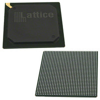
LFE3-150EA-8FN1156C Lattice, LFE3-150EA-8FN1156C Datasheet - Page 44

LFE3-150EA-8FN1156C
Manufacturer Part Number
LFE3-150EA-8FN1156C
Description
IC FPGA 149K LUTS 586I/O FN1156
Manufacturer
Lattice
Series
ECP3r
Datasheets
1.LFE3-150EA-7FN672C.pdf
(136 pages)
2.LFE3-35EA-8FN672I.pdf
(4 pages)
3.LFE3-35EA-8FN672I.pdf
(21 pages)
Specifications of LFE3-150EA-8FN1156C
Number Of Logic Elements/cells
149000
Number Of Labs/clbs
18625
Total Ram Bits
7014400
Number Of I /o
586
Number Of Gates
-
Voltage - Supply
1.14 V ~ 1.26 V
Mounting Type
Surface Mount
Operating Temperature
0°C ~ 85°C
Package / Case
1156-BBGA
Lead Free Status / Rohs Status
Lead free / RoHS Compliant
Available stocks
Company
Part Number
Manufacturer
Quantity
Price
Company:
Part Number:
LFE3-150EA-8FN1156C
Manufacturer:
Transcend
Quantity:
1 000
Part Number:
LFE3-150EA-8FN1156C
Manufacturer:
LATTICE
Quantity:
20 000
Company:
Part Number:
LFE3-150EA-8FN1156CTW
Manufacturer:
Lattice Semiconductor Corporation
Quantity:
10 000
Lattice Semiconductor
Figure 2-38. LatticeECP3 Banks
LatticeECP3 devices contain two types of sysI/O buffer pairs.
1. Top (Bank 0 and Bank 1) and Bottom sysIO Buffer Pairs (Single-Ended Outputs Only)
The sysI/O buffer pairs in the top banks of the device consist of two single-ended output drivers and two sets of
single-ended input buffers (both ratioed and referenced). One of the referenced input buffers can also be con-
figured as a differential input. Only the top edge buffers have a programmable PCI clamp.
The two pads in the pair are described as “true” and “comp”, where the true pad is associated with the positive
side of the differential input buffer and the comp (complementary) pad is associated with the negative side of
the differential input buffer.
The top and bottom sides are ideal for ADDR/CMD signals of DDR3, general purpose I/O, PCI, TR-LVDS (tran-
sition reduced LVDS) or LVDS inputs.
The I/O pins located on the top and bottom sides of the device are fully hot socketable.
V REF1(7)
V REF2(7)
V
V REF1(6)
V REF2(6)
V CCIO6
CCIO7
GND
GND
Bank 0
BOTTOM
SERDES
TOP
Quads
2-41
Bank 1
LatticeECP3 Family Data Sheet
V REF1(2)
V REF2(2)
V CCIO2
GND
V REF1(3)
V REF2(3)
V CCIO3
GND
Architecture


