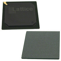
LFE3-150EA-8FN1156C Lattice, LFE3-150EA-8FN1156C Datasheet - Page 28

LFE3-150EA-8FN1156C
Manufacturer Part Number
LFE3-150EA-8FN1156C
Description
IC FPGA 149K LUTS 586I/O FN1156
Manufacturer
Lattice
Series
ECP3r
Datasheets
1.LFE3-150EA-7FN672C.pdf
(136 pages)
2.LFE3-35EA-8FN672I.pdf
(4 pages)
3.LFE3-35EA-8FN672I.pdf
(21 pages)
Specifications of LFE3-150EA-8FN1156C
Number Of Logic Elements/cells
149000
Number Of Labs/clbs
18625
Total Ram Bits
7014400
Number Of I /o
586
Number Of Gates
-
Voltage - Supply
1.14 V ~ 1.26 V
Mounting Type
Surface Mount
Operating Temperature
0°C ~ 85°C
Package / Case
1156-BBGA
Lead Free Status / Rohs Status
Lead free / RoHS Compliant
Available stocks
Company
Part Number
Manufacturer
Quantity
Price
Company:
Part Number:
LFE3-150EA-8FN1156C
Manufacturer:
Transcend
Quantity:
1 000
Part Number:
LFE3-150EA-8FN1156C
Manufacturer:
LATTICE
Quantity:
20 000
Company:
Part Number:
LFE3-150EA-8FN1156CTW
Manufacturer:
Lattice Semiconductor Corporation
Quantity:
10 000
Lattice Semiconductor
MAC DSP Element
In this case, the two operands, AA and AB, are multiplied and the result is added with the previous accumulated
value. This accumulated value is available at the output. The user can enable the input and pipeline registers, but
the output register is always enabled. The output register is used to store the accumulated value. The ALU is con-
figured as the accumulator in the sysDSP slice in the LatticeECP3 family can be initialized dynamically. A regis-
tered overflow signal is also available. The overflow conditions are provided later in this document. Figure 2-27
shows the MAC sysDSP element.
Figure 2-27. MAC DSP Element
DSP Slice
Previous
IR = Input Register
PR = Pipeline Register
OR = Output Register
FR = Flag Register
Rounding
SRIB
SRIA
C_ALU
A_ALU
CIN
0
I
C
IR
AA
MULTA
OR
PR
AMUX
A_ALU
IR
From FPGA Core
AB
To FPGA Core
0
R = Logic (B, C)
R= A ± B ± C
2-25
OR
PR
IR
OPCODE
FR
0
=
=
B_ALU
BMUX
IR
ALU
BA
MULTB
LatticeECP3 Family Data Sheet
PR
OR
IR
BB
IR
COUT
SROB
SROA
DSP Slice
Next
Architecture


