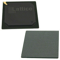
LFE3-150EA-8FN1156C Lattice, LFE3-150EA-8FN1156C Datasheet - Page 6

LFE3-150EA-8FN1156C
Manufacturer Part Number
LFE3-150EA-8FN1156C
Description
IC FPGA 149K LUTS 586I/O FN1156
Manufacturer
Lattice
Series
ECP3r
Datasheets
1.LFE3-150EA-7FN672C.pdf
(136 pages)
2.LFE3-35EA-8FN672I.pdf
(4 pages)
3.LFE3-35EA-8FN672I.pdf
(21 pages)
Specifications of LFE3-150EA-8FN1156C
Number Of Logic Elements/cells
149000
Number Of Labs/clbs
18625
Total Ram Bits
7014400
Number Of I /o
586
Number Of Gates
-
Voltage - Supply
1.14 V ~ 1.26 V
Mounting Type
Surface Mount
Operating Temperature
0°C ~ 85°C
Package / Case
1156-BBGA
Lead Free Status / Rohs Status
Lead free / RoHS Compliant
Available stocks
Company
Part Number
Manufacturer
Quantity
Price
Company:
Part Number:
LFE3-150EA-8FN1156C
Manufacturer:
Transcend
Quantity:
1 000
Part Number:
LFE3-150EA-8FN1156C
Manufacturer:
LATTICE
Quantity:
20 000
Company:
Part Number:
LFE3-150EA-8FN1156CTW
Manufacturer:
Lattice Semiconductor Corporation
Quantity:
10 000
Lattice Semiconductor
Figure 2-2. PFU Diagram
Slice
Slice 0 through Slice 2 contain two LUT4s feeding two registers, whereas Slice 3 contains two LUT4s only. For
PFUs, Slice 0 through Slice 2 can be configured as distributed memory, a capability not available in the PFF.
Table 2-1 shows the capability of the slices in both PFF and PFU blocks along with the operation modes they
enable. In addition, each PFU contains logic that allows the LUTs to be combined to perform functions such as
LUT5, LUT6, LUT7 and LUT8. There is control logic to perform set/reset functions (programmable as synchronous/
asynchronous), clock select, chip-select and wider RAM/ROM functions.
Table 2-1. Resources and Modes Available per Slice
Figure 2-3 shows an overview of the internal logic of the slice. The registers in the slice can be configured for posi-
tive/negative and edge triggered or level sensitive clocks.
Slices 0, 1 and 2 have 14 input signals: 13 signals from routing and one from the carry-chain (from the adjacent
slice or PFU). There are seven outputs: six to routing and one to carry-chain (to the adjacent PFU). Slice 3 has 10
input signals from routing and four signals to routing. Table 2-2 lists the signals associated with Slice 0 to Slice 2.
Slice 0
Slice 1
Slice 2
Slice 3
Slice
2 LUT4s and 2 Registers Logic, Ripple, RAM, ROM 2 LUT4s and 2 Registers
2 LUT4s and 2 Registers Logic, Ripple, RAM, ROM 2 LUT4s and 2 Registers
2 LUT4s and 2 Registers Logic, Ripple, RAM, ROM 2 LUT4s and 2 Registers
FF
LUT4 &
CARRY
D
Slice 0
Resources
2 LUT4s
FF
LUT4 &
CARRY
D
PFU BLock
FF
LUT4 &
CARRY
D
Slice 1
Logic, ROM
Modes
LUT4 &
CARRY
FF
D
Routing
Routing
From
2-3
To
FF
CARRY
LUT4 &
D
Slice 2
Resources
2 LUT4s
FF
CARRY
LUT4 &
D
LatticeECP3 Family Data Sheet
PFF Block
LUT4
Slice 3
Logic, Ripple, ROM
Logic, Ripple, ROM
Logic, Ripple, ROM
Logic, ROM
LUT4
Modes
Architecture


