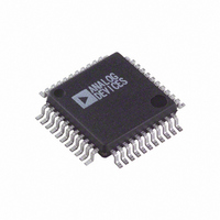
AD7841AS Analog Devices Inc, AD7841AS Datasheet - Page 12

AD7841AS
Manufacturer Part Number
AD7841AS
Description
IC DAC 14BIT OCTAL VOUT 44-MQFP
Manufacturer
Analog Devices Inc
Datasheet
1.AD7841ASZ-REEL.pdf
(13 pages)
Specifications of AD7841AS
Rohs Status
RoHS non-compliant
Settling Time
31µs
Number Of Bits
14
Data Interface
Parallel
Number Of Converters
8
Voltage Supply Source
Analog and Digital, Dual ±
Power Dissipation (max)
303mW
Operating Temperature
-40°C ~ 85°C
Mounting Type
Surface Mount
Package / Case
44-MQFP, 44-PQFP
For Use With
EVAL-AD7841EBZ - BOARD EVAL FOR AD7841
Available stocks
Company
Part Number
Manufacturer
Quantity
Price
Company:
Part Number:
AD7841AS
Manufacturer:
AD
Quantity:
5 510
Company:
Part Number:
AD7841ASZ
Manufacturer:
Analog Devices Inc
Quantity:
10 000
Part Number:
AD7841ASZ
Manufacturer:
ADI/亚德诺
Quantity:
20 000
Company:
Part Number:
AD7841ASZ-REEL
Manufacturer:
Analog Devices Inc
Quantity:
10 000
AD7841
The AD8803 has an output voltage range of GND to V
to 5 V). To trim the V
on the AD8803 DAC can be set using the V
allowing 8 bits of resolution between the two points. This will
allow the V
To trim the V
voltage in the required negative voltage range is required. Neither
the AD7804 or the AD8803 can provide this range in normal
operation as their output range is 0 V to 5 V. There are two
methods of producing this negative voltage. One method is to
REF
REF
(+) pin to be adjusted to remove gain errors.
(–) voltage, some method of providing a trim
CONTROLLER
ADDR BUS
DATA BUS
REF
SDATA
(+) input, the appropriate trim range
SCLK
LOGIC LEVEL
SHIFT
DECODER
ADDR
REFL
ADDITIONAL PINS OMITTED FOR CLARITY
FSIN/CS
FSIN/CS
and V
SCLK
SCLK
D IN
D IN
REFH
DD
8/10-BIT
8/10-BIT
DAC
DAC
(0 V
pins
+5V
GND
GND
V
V
5V
DD
DD
provide a positive output voltage and then to level shift that ana-
log voltage to the required negative range. Alternatively these
DACs can be operated with supplies of 0 V and –5 V, with the
V
Now these can be used to provide the negative reference volt-
ages for the V
signals driving the DACs need to be level-shifted from the 0 V
to +5 V range to the –5 V to 0 V range. Figure 13 shows a
typical application circuit to provide programmable reference
capabilities for the AD7841.
DD
pin connected to 0 V and the GND pin connected to –5 V.
0V TO
0V TO +5V
REF
5V
(–) inputs on the AD7841. However, the digital
V
V
DATA BUS
REF
REF
( )AB
(+)AB
AD7841
A0, A1, A2
GND
V
V
OUT
OUT
A
B
V
V
OUT
OUT
A
B
REV. B


