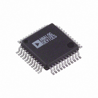
AD7841AS Analog Devices Inc, AD7841AS Datasheet - Page 6

AD7841AS
Manufacturer Part Number
AD7841AS
Description
IC DAC 14BIT OCTAL VOUT 44-MQFP
Manufacturer
Analog Devices Inc
Datasheet
1.AD7841ASZ-REEL.pdf
(13 pages)
Specifications of AD7841AS
Rohs Status
RoHS non-compliant
Settling Time
31µs
Number Of Bits
14
Data Interface
Parallel
Number Of Converters
8
Voltage Supply Source
Analog and Digital, Dual ±
Power Dissipation (max)
303mW
Operating Temperature
-40°C ~ 85°C
Mounting Type
Surface Mount
Package / Case
44-MQFP, 44-PQFP
For Use With
EVAL-AD7841EBZ - BOARD EVAL FOR AD7841
Available stocks
Company
Part Number
Manufacturer
Quantity
Price
Company:
Part Number:
AD7841AS
Manufacturer:
AD
Quantity:
5 510
Company:
Part Number:
AD7841ASZ
Manufacturer:
Analog Devices Inc
Quantity:
10 000
Part Number:
AD7841ASZ
Manufacturer:
ADI/亚德诺
Quantity:
20 000
Company:
Part Number:
AD7841ASZ-REEL
Manufacturer:
Analog Devices Inc
Quantity:
10 000
AD7841
TERMINOLOGY
Relative Accuracy
Relative accuracy or endpoint linearity is a measure of the max-
imum deviation from a straight line passing through the endpoints
of the DAC transfer function. It is measured after adjusting for
zero-scale error and full-scale error and is expressed in Least
Significant Bits.
Differential Nonlinearity
Differential nonlinearity is the difference between the measured
change and the ideal 1 LSB change between any two adjacent
codes. A specified differential nonlinearity of 1 LSB maximum
ensures monotonicity.
DC Crosstalk
Although the common input reference voltage signals are inter-
nally buffered, small IR drops in the individual DAC reference
inputs across the die can mean that an update to one channel
can produce a dc output change in one or another of the chan-
nel outputs.
The eight DAC outputs are buffered by op amps that share
common V
changes in one channel (due to an update), this can result in a
further dc change in one or another of the channel outputs. This
effect is most obvious at high load currents and reduces as the
load currents are reduced. With high impedance loads the effect
is virtually impossible to measure.
Output Voltage Settling Time
This is the amount of time it takes for the output to settle to a
specified level for a full-scale input change.
Digital-to-Analog Glitch Impulse
This is the amount of charge injected into the analog output
when the inputs change state. It is specified as the area of the
glitch in nV-secs. It is measured with V
V
and 2000H.
Channel-to-Channel Isolation
Channel-to-channel isolation refers to the proportion of input
signal from one DAC’s reference input that appears at the out-
put of another DAC. It is expressed in dBs.
DAC-to-DAC Crosstalk
DAC-to-DAC crosstalk is defined as the glitch impulse that
appears at the output of one converter due to both the digital
change and subsequent analog O/P change at another converter.
It is specified in nV-secs.
Digital Crosstalk
The glitch impulse transferred to the output of one converter
due to a change in digital input code to the other converter is
defined as the digital crosstalk and is specified in nV-secs.
Digital Feedthrough
When the device is not selected, high frequency logic activity on
the device’s digital inputs can be capacitively coupled both
across and through the device to show up as noise on the V
pins. This noise is digital feedthrough.
REF
(–) = –5 V and the digital inputs toggled between 1FFFH
DD
and V
SS
power supplies. If the dc load current
REF
(+) = +5 V and
OUT
DC Output Impedance
This is the effective output source resistance. It is dominated by
package lead resistance.
Full-Scale Error
This is the error in DAC output voltage when all 1s are loaded
into the DAC latch. Ideally the output voltage, with all 1s loaded
into the DAC latch, should be 2 V
Zero-Scale Error
Zero-scale error is the error in the DAC output voltage when all
0s are loaded into the DAC latch. Ideally the output voltage,
with all 0s in the DAC latch should be equal to 2 V
scale error is mainly due to offsets in the output amplifier.
Gain Error
Gain Error is defined as (Full-Scale Error) – (Zero-Scale Error).
GENERAL DESCRIPTION
DAC Architecture—General
Each channel consists of a straight 14-bit R-2R voltage-mode
DAC. The full-scale output voltage range is equal to twice the
reference span of V
binary; all 0s produces an output of 2 V
an output of 2 V
The analog output voltage of each DAC channel reflects the
contents of its own DAC register. Data is transferred from
the external bus to the input register of each DAC on a per
channel basis.
Bringing the CLR line low switches all the signal outputs, V
to V
When the CLR signal is brought back high, the output voltages
from the DACs will reflect the data stored in the relevant
DAC registers.
Data Loading to the AD7841
Data is loaded into the AD7841 in straight parallel 14-bit wide
words.
The DAC output voltages, V
reflect new data in the DAC registers.
The actual input register being written to is determined by the
logic levels present on the device’s address lines, as shown in
Table I.
A2
0
0
0
0
1
1
1
1
OUT
H, to the voltage level on the relevant DUTGND pin.
A1
0
0
1
1
0
0
1
1
Table I. Address Line Truth Table
REF
REF
(+) – 1 LSB.
(+) – V
A0
0
1
0
1
0
1
0
1
REF
OUT
(–). The DAC coding is straight
A – V
REF
(+) – 1 LSB.
DAC Selected
INPUT REG A (DAC A)
INPUT REG B (DAC B)
INPUT REG C (DAC C)
INPUT REG D (DAC D)
INPUT REG E (DAC E)
INPUT REG F (DAC F)
INPUT REG G (DAC G)
INPUT REG H (DAC H)
OUT
REF
H are updated to
(–); all 1s produces
REF
(–). Zero-
REV. B
OUT
A


