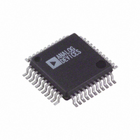
AD7841AS Analog Devices Inc, AD7841AS Datasheet - Page 8

AD7841AS
Manufacturer Part Number
AD7841AS
Description
IC DAC 14BIT OCTAL VOUT 44-MQFP
Manufacturer
Analog Devices Inc
Datasheet
1.AD7841ASZ-REEL.pdf
(13 pages)
Specifications of AD7841AS
Rohs Status
RoHS non-compliant
Settling Time
31µs
Number Of Bits
14
Data Interface
Parallel
Number Of Converters
8
Voltage Supply Source
Analog and Digital, Dual ±
Power Dissipation (max)
303mW
Operating Temperature
-40°C ~ 85°C
Mounting Type
Surface Mount
Package / Case
44-MQFP, 44-PQFP
For Use With
EVAL-AD7841EBZ - BOARD EVAL FOR AD7841
Available stocks
Company
Part Number
Manufacturer
Quantity
Price
Company:
Part Number:
AD7841AS
Manufacturer:
AD
Quantity:
5 510
Company:
Part Number:
AD7841ASZ
Manufacturer:
Analog Devices Inc
Quantity:
10 000
Part Number:
AD7841ASZ
Manufacturer:
ADI/亚德诺
Quantity:
20 000
Company:
Part Number:
AD7841ASZ-REEL
Manufacturer:
Analog Devices Inc
Quantity:
10 000
AD7841
Unipolar Configuration
Figure 2 shows the AD7841 in the unipolar binary circuit
configuration. The V
AD586, a 5 V reference. V
gives the code table for unipolar operation of the AD7841.
Other suitable references include the REF02, a precision 5 V
reference, and the REF195, a low dropout, micropower preci-
sion 5 V reference.
Offset and gain may be adjusted in Figure 2 as follows: To
adjust offset, disconnect the V
DAC with all 0s and adjust the V
For gain adjustment, the AD7841 should be loaded with all 1s
and R1 adjusted until V
16384) = 9.99939 V.
Many circuits will not require these offset and gain adjustments.
In these circuits R1 can be omitted. Pin 5 of the AD586 may be
left open circuit and Pin 2 (V
Binary Number in DAC Register
MSB
NOTES
V= V
For V
Bipolar Configuration
Figure 3 shows the AD7841 set up for ± 10 V operation. The
AD588 provides precision ± 5 V tracking outputs that are fed to
the V
for bipolar operation of the AD7841 is shown in Table III.
In Figure 3, full-scale and bipolar zero adjustments are provided
by varying the gain and balance on the AD588. R2 varies the
gain on the AD588 while R3 adjusts the offset of both the +5 V
and –5 V outputs together with respect to ground.
For bipolar-zero adjustment, the DAC is loaded with
1000 . . . 0000 and R3 is adjusted until V
is adjusted by loading the DAC with all 1s and adjusting R2
until V
11
10
01
00
00
REF
REF
1 F
REF
C1
(+); V
OUT
(+) = 5 V, 1 LSB = 10 V/2
1111
0000
1111
0000
0000
(+) and V
Table II. Code Table for Unipolar Operation
8
= 10(8191/8192) V = 9.99878 V.
REF
SIGNAL
AD586
GND
(–) = 0 V for unipolar operation.
4
2
ADDITIONAL PINS OMITTED FOR CLARITY
1111
0000
1111
0000
0000
REF
6
5
REF
(–) inputs of the AD7841. The code table
OUT
(+) input of the DAC is driven by the
R1
10k
1111
0000
1111
0001
0000
REF
LSB
= 2 V
14
REF
(–) is tied to ground. Table II
REF
= 10 V/16384 = 610 µV.
V
V
REF
REF
REF
(–)) of the AD7841 tied to 0 V.
REF
+15V
V
(–) input from 0 V, load the
AD7841
DD
(+)
(–)
(–) voltage until V
(+) – 1 LSB = 10 V(16383/
–15V
V
SS
DUTGND
+5V
V
Analog Output
(V
2 V
2 V
2 V
2 V
0 V
CC
V
GND
OUT
OUT
OUT
REF
REF
REF
REF
)
(16383/16384) V
(8192/16384) V
(8191/16384) V
(1/16384) V
= 0 V. Full scale
SIGNAL
GND
V
(0 TO +10V)
OUT
OUT
= 0 V.
When bipolar-zero and full-scale adjustment are not needed, R2
and R3 can be omitted. Pin 12 on the AD588 should be con-
nected to Pin 11 and Pin 5 should be left floating.
Binary Number in DAC
Register
MSB
11
10
10
01
00
00
NOTES
V
For V
20 V/16384 = 1.22 mV.
CONTROLLED POWER-ON OF THE OUTPUT STAGE
A block diagram of the output stage of the AD7841 is shown in
Figure 4. It is capable of driving a load of 5 kΩ in parallel with
50 pF. G
power on voltage present at V
also used in conjunction with the CLR input to set V
user defined voltage present at the DUTGND pin. When CLR
is taken back high, the DAC outputs reflect the data in the
DAC registers.
100k
REF
R2
= (V
REF
1111 1111 1111
0000 0000 0001
0000 0000 0000
1111 1111 1111
0000 0000 0001
0000 0000 0000
100k
(+) = +5 V, and V
REF
DAC
R3
Table III. Code Table for Bipolar Operation
1
1 F
(+) – V
C1
to G
10
11
7
9
5
REF
6
12 8 13
are transmission gates used to control the
G
G
(–)).
1
AD588
ADDITIONAL PINS OMITTED FOR CLARITY
2
4
LSB
REF
DUTGND
6
39k
R
(–) = –5 V, V
R1
2
3
1
14
15
16
G
Analog Output
(V
2[V
2[V
2[V
2[V
2[V
2[V
4
OUT
OUT
G
G
REF
REF
REF
REF
REF
REF
V
V
R = 60k
±
3
5
. On power up G
REF
REF
+15V
)
REF
V
(–) + V
(–) + V
(–) + V
(–) + V
(–) + V
(–)] V
AD7841
(+)
(–)
DD
14k
–15V
= 10 V, 1 LSB = 2 V
V
SS
DUTGND
G
+5V
6
V
CC
REF
REF
REF
REF
REF
V
GND
OUT
(16383/16384)] V
(8193/16384)] V
(8192/16384)] V
(8191/16384)] V
(1/16384)] V
SIGNAL
1
GND
and G
V
(–10V TO +10V)
OUT
OUT
V
OUT
REF
REV. B
to the
V/2
2
are
14
=


