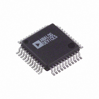
AD7841AS Analog Devices Inc, AD7841AS Datasheet - Page 2

AD7841AS
Manufacturer Part Number
AD7841AS
Description
IC DAC 14BIT OCTAL VOUT 44-MQFP
Manufacturer
Analog Devices Inc
Datasheet
1.AD7841ASZ-REEL.pdf
(13 pages)
Specifications of AD7841AS
Rohs Status
RoHS non-compliant
Settling Time
31µs
Number Of Bits
14
Data Interface
Parallel
Number Of Converters
8
Voltage Supply Source
Analog and Digital, Dual ±
Power Dissipation (max)
303mW
Operating Temperature
-40°C ~ 85°C
Mounting Type
Surface Mount
Package / Case
44-MQFP, 44-PQFP
For Use With
EVAL-AD7841EBZ - BOARD EVAL FOR AD7841
Available stocks
Company
Part Number
Manufacturer
Quantity
Price
Company:
Part Number:
AD7841AS
Manufacturer:
AD
Quantity:
5 510
Company:
Part Number:
AD7841ASZ
Manufacturer:
Analog Devices Inc
Quantity:
10 000
Part Number:
AD7841ASZ
Manufacturer:
ADI/亚德诺
Quantity:
20 000
Company:
Part Number:
AD7841ASZ-REEL
Manufacturer:
Analog Devices Inc
Quantity:
10 000
AD7841–SPECIFICATIONS
Parameter
ACCURACY
REFERENCE INPUTS
DUTGND INPUTS
OUTPUT CHARACTERISTICS
DIGITAL INPUTS
POWER REQUIREMENTS
NOTES
1
2
3
4
Specifications subject to change without notice.
See DUTGND Voltage Range section.
Temperature range for A and B Versions: –40°C to +85°C.
Guaranteed by characterization. Not production tested.
The AD7841 is functional with power supplies of ± 12 V ± 10% with reduced output range. Output amplifier requires 2.5 V of head room at the bottom and top ends
of the transfer for function. At 12 V supplies it is recommended to restrict the reference range to ± 4 V.
Resolution
Relative Accuracy
Differential Nonlinearity
Zero-Scale Error
Full-Scale Error
Gain Error
Gain Temperature Coefficient
DC Crosstalk
DC Input Impedance
Input Current
V
V
[V
DC Input Impedance
Max Input Current
Input Range
Output Voltage Swing
Short Circuit Current
Resistive Load
Capacitive Load
DC Output Impedance
V
V
I
C
V
V
V
Power Supply Sensitivity
I
I
I
INH
CC
DD
SS
REF
REF
INH
INL
CC
DD
SS
IN
REF
@ 25°C
T
∆Full Scale/∆V
∆Full Scale/∆V
, Input Capacitance
, Input Current
MIN
, Input Low Voltage
(+) Range
(–) Range
, Input High Voltage
(+) – V
to T
3
MAX
REF
2
(–)]
DD
SS
2
2
2
2
4
2
2
A
14
± 4
–0.9/2
± 8
± 8
± 2
0.5
10
120
100
± 1
0/5
–5/0
2/10
60
± 0.3
–2/+2
V
V
15
5
50
0.5
2.4
0.8
± 1
± 10
10
4.75/+5.25
15 V ± 10%
–15 V ± 10%
90
90
0.5
10
10
SS
DD
+ 2.5 V to
– 2.5 V
B
14
± 2
± 1
± 8
± 8
± 2
0.5
10
120
100
± 1
0/5
–5/0
2/10
60
± 0.3
–2/+2
V
V
15
5
50
0.5
2.4
0.8
± 1
± 10
10
4.75/+5.25
15 V ± 10%
–15 V ± 10%
90
90
0.5
10
10
SS
DD
(V
0 V; R
CC
+ 2.5 V to
– 2.5 V
= 5 V
L
= 5 k
5%; V
V min/max
and C
Unit
Bits
LSB max
LSB max
LSB max
LSB max
LSB typ
ppm FSR/°C typ
ppm FSR/°C max
µV max
MΩ typ
µA max
V min/max
V min/max
V min/max
kΩ typ
mA typ
V min/max
V typ
mA max
kΩ min
pF max
Ω max
V min
V max
µA max
µA max
pF max
V min/max
V min/max
dB typ
dB typ
mA max
mA max
mA max
DD
= 15 V
L
= 50 pF to GND, T
10%; V
Test Conditions/Comments
Guaranteed Monotonic Over Temperature for All
Grades
V
±2 LSB
V
±2 LSB
V
See Terminology. Typically 75 µV
Per Input. Typically ± 0.03 µA
For Specified Performance. Can Go as Low as 0 V,
Per Input
V
– V
To 0 V
To 0 V
Total for All Pins
For Specified Performance
For Specified Performance
For Specified Performance
V
Outputs Unloaded. Typically 8 mA
Outputs Unloaded. Typically 8 mA
but Performance Not Guaranteed
REF
REF
REF
OUT
INH
SS
DUTGND
= –15 V
A
(+) = +5 V, V
(+) = +5 V, V
(+) = +5 V, V
1
= V
= 2 × (V
= T
CC
MIN
, V
to T
REF
INL
10%; GND = DUTGND =
MAX
(–) + [V
= GND. Dynamic Current
REF
REF
REF
, unless otherwise noted)
(–) = –5 V. Typically within
(–) = –5 V. Typically within
(–) = –5 V
REF
(+) – V
REF
(–)] × D)
REV. B


