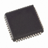
ATF1502ASL-25JU44 Atmel, ATF1502ASL-25JU44 Datasheet - Page 9

ATF1502ASL-25JU44
Manufacturer Part Number
ATF1502ASL-25JU44
Description
IC CPLD EE LP 25NS 44-PLCC
Manufacturer
Atmel
Series
ATF1502AS(L)r
Datasheet
1.ATF1502ASL-25JU44.pdf
(26 pages)
Specifications of ATF1502ASL-25JU44
Programmable Type
In System Programmable (min 10K program/erase cycles)
Delay Time Tpd(1) Max
25.0ns
Voltage Supply - Internal
4.5 V ~ 5.5 V
Number Of Macrocells
32
Number Of I /o
32
Operating Temperature
-40°C ~ 85°C
Mounting Type
Surface Mount
Package / Case
44-PLCC
Voltage
4.75 V ~ 5.25 V
Memory Type
EEPROM
Family Name
ATF1502ASL
# Macrocells
32
Number Of Usable Gates
750
Frequency (max)
60MHz
Propagation Delay Time
25ns
Number Of Logic Blocks/elements
2
# I/os (max)
32
Operating Supply Voltage (typ)
5V
In System Programmable
Yes
Operating Supply Voltage (min)
4.5V
Operating Supply Voltage (max)
5.5V
Operating Temp Range
-40C to 85C
Operating Temperature Classification
Industrial
Mounting
Surface Mount
Pin Count
44
Package Type
PLCC
Number Of Product Terms Per Macro
40
Maximum Operating Frequency
60 MHz
Delay Time
25 ns
Number Of Programmable I/os
32
Operating Supply Voltage
5 V
Maximum Operating Temperature
+ 85 C
Minimum Operating Temperature
- 40 C
Mounting Style
SMD/SMT
Supply Voltage (max)
5.5 V
Supply Voltage (min)
4.5 V
For Use With
ATF15XX-DK3 - KIT DEV FOR ATF15XX CPLD'S
Lead Free Status / RoHS Status
Lead free / RoHS Compliant
Features
-
Number Of Logic Elements/cells
-
Lead Free Status / Rohs Status
Compliant
Available stocks
Company
Part Number
Manufacturer
Quantity
Price
JTAG
Boundary-scan
Cell (BSC)
Testing
BSC
Configuration
for Input and I/O
Pins (Except
JTAG TAP Pins)
BSC
Configuration
for Macrocell
0995K–PLD–6/05
The ATF1502AS contains up to 32 I/O pins and four input pins, depending on the device type
and package type selected. Each input pin and I/O pin has its own boundary-scan cell (BSC)
in order to support boundary-scan testing as described in detail by IEEE Standard 1149.1. A
typical BSC consists of three capture registers or scan registers and up to two update regis-
ters. There are two types of BSCs, one for input or I/O pin, and one for the macrocells. The
BSCs in the device are chained together through the capture registers. Input to the capture
register chain is fed in from the TDI pin while the output is directed to the TDO pin. Capture
registers are used to capture active device data signals, to shift data in and out of the device
and to load data into the update registers. Control signals are generated internally by the
JTAG TAP controller. The BSC configuration for the input and I/O pins and macrocells is
shown below.
Note:
1. The ATF1502AS has a pull-up option on TMS and TDI pins. This feature is selected as a
design option.
TDO
Q
OEJ
OUTJ
TDI
D
CLOCK
Shift
1
1
0
0
0
1
BSC for I/O Pins and Macrocells
TDI
Capture
D Q
D Q
DR
TDO
Clock
Update
D Q
D Q
DR
1
1
0
0
Mode
ATF1502AS(L)
Pin
9


