EPM570F100C4N Altera, EPM570F100C4N Datasheet - Page 39
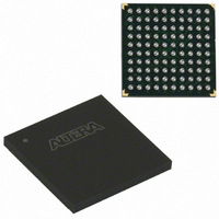
EPM570F100C4N
Manufacturer Part Number
EPM570F100C4N
Description
IC MAX II CPLD 570 LE 100-FBGA
Manufacturer
Altera
Series
MAX® IIr
Specifications of EPM570F100C4N
Programmable Type
In System Programmable
Delay Time Tpd(1) Max
5.4ns
Voltage Supply - Internal
2.5V, 3.3V
Number Of Logic Elements/blocks
570
Number Of Macrocells
440
Number Of I /o
76
Operating Temperature
0°C ~ 85°C
Mounting Type
Surface Mount
Package / Case
100-FBGA
Voltage
2.5V, 3.3V
Memory Type
FLASH
Number Of Logic Elements/cells
570
Family Name
MAX II
# Macrocells
440
Frequency (max)
2.3148GHz
Propagation Delay Time
7ns
Number Of Logic Blocks/elements
57
# I/os (max)
76
Operating Supply Voltage (typ)
2.5/3.3V
In System Programmable
Yes
Operating Supply Voltage (min)
2.375V
Operating Supply Voltage (max)
3.6V
Operating Temp Range
0C to 85C
Operating Temperature Classification
Commercial
Mounting
Surface Mount
Pin Count
100
Package Type
FBGA
No. Of I/o's
76
Propagation Delay
7ns
Global Clock Setup Time
1.5ns
Frequency
247.5MHz
Supply Voltage Range
2.375V To 2.625V, 3V To 3.6V
Operating Temperature Range
0°C To +85°C
Rohs Compliant
Yes
Lead Free Status / RoHS Status
Lead free / RoHS Compliant
Features
-
Lead Free Status / Rohs Status
Compliant
Other names
544-1716
Available stocks
Company
Part Number
Manufacturer
Quantity
Price
Company:

Part Number:
EPM570F100C4N
Manufacturer:
ALTERA
Quantity:
12 388
Company:
Part Number:
EPM570F100C4N
Manufacturer:
ALTERA
Quantity:
325
Part Number:
EPM570F100C4N
Manufacturer:
ALTERA/阿尔特拉
Quantity:
20 000


Chapter 2: MAX II Architecture
I/O Structure
Bus Hold
Programmable Pull-Up Resistor
Programmable Input Delay
MultiVolt I/O Interface
© October 2008 Altera Corporation
1
Each MAX II device I/O pin provides an optional bus-hold feature. The bus-hold
circuitry can hold the signal on an I/O pin at its last-driven state. Since the bus-hold
feature holds the last-driven state of the pin until the next input signal is present, an
external pull-up or pull-down resistor is not necessary to hold a signal level when the
bus is tri-stated.
The bus-hold circuitry also pulls undriven pins away from the input threshold
voltage where noise can cause unintended high-frequency switching. The designer
can select this feature individually for each I/O pin. The bus-hold output will drive
no higher than V
the device cannot use the programmable pull-up option.
The bus-hold circuitry uses a resistor to pull the signal level to the last driven state.
The
specific sustaining current for each V
overdrive current used to identify the next-driven input level.
The bus-hold circuitry is only active after the device has fully initialized. The bus-hold
circuit captures the value on the pin present at the moment user mode is entered.
Each MAX II device I/O pin provides an optional programmable pull-up resistor
during user mode. If the designer enables this feature for an I/O pin, the pull-up
resistor holds the output to the V
The programmable pull-up resistor feature should not be used at the same time as the
bus-hold feature on a given I/O pin.
The MAX II IOE includes a programmable input delay that is activated to ensure zero
hold times. A path where a pin directly drives a register, with minimal routing
between the two, may require the delay to ensure zero hold time. However, a path
where a pin drives a register through long routing or through combinational logic
may not require the delay to achieve a zero hold time. The Quartus II software uses
this delay to ensure zero hold times when needed.
The MAX II architecture supports the MultiVolt I/O interface feature, which allows
MAX II devices in all packages to interface with systems of different supply voltages.
The devices have one set of VCC pins for internal operation (V
sets for input buffers and I/O output driver buffers (V
of I/O banks available in the devices where each set of VCC pins powers one I/O
bank. The EPM240 and EPM570 devices have two I/O banks respectively while the
EPM1270 and EPM2210 devices have four I/O banks respectively.
DC and Switching Characteristics
CCIO
to prevent overdriving signals. If the bus-hold feature is enabled,
CCIO
chapter in the MAX II Device Handbook gives the
CCIO
level of the output pin’s bank.
voltage level driven through this resistor and
CCIO
), depending on the number
CCINT
), and up to four
MAX II Device Handbook
2–31
Related parts for EPM570F100C4N
Image
Part Number
Description
Manufacturer
Datasheet
Request
R

Part Number:
Description:
CYCLONE II STARTER KIT EP2C20N
Manufacturer:
Altera
Datasheet:


Part Number:
Description:
CPLD, EP610 Family, ECMOS Process, 300 Gates, 16 Macro Cells, 16 Reg., 16 User I/Os, 5V Supply, 35 Speed Grade, 24DIP
Manufacturer:
Altera Corporation
Datasheet:
Part Number:
Description:
CPLD, EP610 Family, ECMOS Process, 300 Gates, 16 Macro Cells, 16 Reg., 16 User I/Os, 5V Supply, 15 Speed Grade, 24DIP
Manufacturer:
Altera Corporation
Datasheet:
Part Number:
Description:
Manufacturer:
Altera Corporation
Datasheet:
Part Number:
Description:
CPLD, EP610 Family, ECMOS Process, 300 Gates, 16 Macro Cells, 16 Reg., 16 User I/Os, 5V Supply, 30 Speed Grade, 24DIP
Manufacturer:
Altera Corporation
Datasheet:
Part Number:
Description:
High-performance, low-power erasable programmable logic devices with 8 macrocells, 10ns
Manufacturer:
Altera Corporation
Datasheet:
Part Number:
Description:
High-performance, low-power erasable programmable logic devices with 8 macrocells, 7ns
Manufacturer:
Altera Corporation
Datasheet:
Part Number:
Description:
Classic EPLD
Manufacturer:
Altera Corporation
Datasheet:
Part Number:
Description:
High-performance, low-power erasable programmable logic devices with 8 macrocells, 10ns
Manufacturer:
Altera Corporation
Datasheet:
Part Number:
Description:
Manufacturer:
Altera Corporation
Datasheet:
Part Number:
Description:
Manufacturer:
Altera Corporation
Datasheet:
Part Number:
Description:
Manufacturer:
Altera Corporation
Datasheet:
Part Number:
Description:
CPLD, EP610 Family, ECMOS Process, 300 Gates, 16 Macro Cells, 16 Reg., 16 User I/Os, 5V Supply, 25 Speed Grade, 24DIP
Manufacturer:
Altera Corporation
Datasheet: