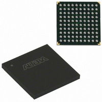
EPM570F100C4N Altera, EPM570F100C4N Datasheet - Page 49

EPM570F100C4N
Manufacturer Part Number
EPM570F100C4N
Description
IC MAX II CPLD 570 LE 100-FBGA
Manufacturer
Altera
Series
MAX® IIr
Specifications of EPM570F100C4N
Programmable Type
In System Programmable
Delay Time Tpd(1) Max
5.4ns
Voltage Supply - Internal
2.5V, 3.3V
Number Of Logic Elements/blocks
570
Number Of Macrocells
440
Number Of I /o
76
Operating Temperature
0°C ~ 85°C
Mounting Type
Surface Mount
Package / Case
100-FBGA
Voltage
2.5V, 3.3V
Memory Type
FLASH
Number Of Logic Elements/cells
570
Family Name
MAX II
# Macrocells
440
Frequency (max)
2.3148GHz
Propagation Delay Time
7ns
Number Of Logic Blocks/elements
57
# I/os (max)
76
Operating Supply Voltage (typ)
2.5/3.3V
In System Programmable
Yes
Operating Supply Voltage (min)
2.375V
Operating Supply Voltage (max)
3.6V
Operating Temp Range
0C to 85C
Operating Temperature Classification
Commercial
Mounting
Surface Mount
Pin Count
100
Package Type
FBGA
No. Of I/o's
76
Propagation Delay
7ns
Global Clock Setup Time
1.5ns
Frequency
247.5MHz
Supply Voltage Range
2.375V To 2.625V, 3V To 3.6V
Operating Temperature Range
0°C To +85°C
Rohs Compliant
Yes
Lead Free Status / RoHS Status
Lead free / RoHS Compliant
Features
-
Lead Free Status / Rohs Status
Compliant
Other names
544-1716
Available stocks
Company
Part Number
Manufacturer
Quantity
Price
Company:
Part Number:
EPM570F100C4N
Manufacturer:
ALTERA
Quantity:
12 388
Company:
Part Number:
EPM570F100C4N
Manufacturer:
ALTERA
Quantity:
325
Part Number:
EPM570F100C4N
Manufacturer:
ALTERA/阿尔特拉
Quantity:
20 000
Chapter 3: JTAG and In-System Programmability
Referenced Documents
Real-Time ISP
Design Security
Programming with External Hardware
Referenced Documents
© October 2008 Altera Corporation
For systems that require more than DC logic level control of I/O pins, the real-time
ISP feature allows you to update the CFM block with a new design image while the
current design continues to operate in the SRAM logic array and I/O pins. A new
programming file is updated into the MAX II device without halting the original
design’s operation, saving down-time costs for remote or field upgrades. The updated
CFM block configures the new design into the SRAM upon the next power cycle. It is
also possible to execute an immediate configuration of the SRAM without a power
cycle by using a specific sequence of ISP commands. The configuration of SRAM
without a power cycle takes a specific amount of time (t
I/O pins are tri-stated and weakly pulled-up to V
All MAX II devices contain a programmable security bit that controls access to the
data programmed into the CFM block. When this bit is programmed, design
programming information, stored in the CFM block, cannot be copied or retrieved.
This feature provides a high level of design security because programmed data within
flash memory cells is invisible. The security bit that controls this function, as well as
all other programmed data, is reset only when the device is erased. The SRAM is also
invisible and cannot be accessed regardless of the security bit setting. The UFM block
data is not protected by the security bit and is accessible through JTAG or logic array
connections.
MAX II devices can be programmed by downloading the information via in-circuit
testers, embedded processors, the Altera
ByteBlaster™ II, and USB-Blaster cables.
BP Microsystems, System General, and other programming hardware manufacturers
provide programming support for Altera devices. Check their websites for device
support information.
This chapter references the following documents:
■
■
■
■
DC and Switching Characteristics
IEEE 1149.1 (JTAG) Boundary-Scan Testing for MAX II Devices
Device Handbook
Real-Time ISP and ISP Clamp for MAX II Devices
Handbook
Using Jam STAPL for ISP via an Embedded Processor
Handbook
chapter in the MAX II Device Handbook
®
ByteblasterMV™, MasterBlaster™,
CCIO
chapter in the MAX II Device
.
chapter in the MAX II Device
CONFIG
). During this time, the
chapter in the MAX II
MAX II Device Handbook
3–7


