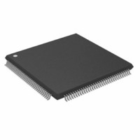
ADSP-21261SKSTZ150 Analog Devices Inc, ADSP-21261SKSTZ150 Datasheet - Page 21

ADSP-21261SKSTZ150
Manufacturer Part Number
ADSP-21261SKSTZ150
Description
IC DSP 32BIT 150MHZ 144LQFP
Manufacturer
Analog Devices Inc
Series
SHARC®r
Type
Fixed/Floating Pointr
Specifications of ADSP-21261SKSTZ150
Interface
DAI, SPI
Clock Rate
150MHz
Non-volatile Memory
ROM (384 kB)
On-chip Ram
128kB
Voltage - I/o
3.30V
Voltage - Core
1.20V
Operating Temperature
0°C ~ 70°C
Mounting Type
Surface Mount
Package / Case
144-LQFP
No. Of Bits
32 / 40
Frequency
150MHz
Supply Voltage
1.2V
Embedded Interface Type
Serial
Supply Voltage Range
1.14V To 1.26V
Operating Temperature Range
0°C To +70°C
Digital Ic
RoHS Compliant
Device Core Size
32/40Bit
Architecture
Super Harvard
Format
Floating Point
Clock Freq (max)
150MHz
Mips
150
Device Input Clock Speed
150MHz
Ram Size
128KB
Program Memory Size
384KB
Operating Supply Voltage (typ)
1.2/3.3V
Operating Supply Voltage (min)
1.14/3.13V
Operating Supply Voltage (max)
1.26/3.47V
Operating Temp Range
0C to 70C
Operating Temperature Classification
Commercial
Mounting
Surface Mount
Pin Count
144
Package Type
LQFP
Package
144LQFP
Numeric And Arithmetic Format
Floating-Point
Maximum Speed
150 MHz
Device Million Instructions Per Second
150 MIPS
Lead Free Status / RoHS Status
Lead free / RoHS Compliant
Lead Free Status / RoHS Status
Lead free / RoHS Compliant
Available stocks
Company
Part Number
Manufacturer
Quantity
Price
Company:
Part Number:
ADSP-21261SKSTZ150
Manufacturer:
Analog Devices Inc
Quantity:
10 000
Part Number:
ADSP-21261SKSTZ150
Manufacturer:
ADI/亚德诺
Quantity:
20 000
Timer PWM_OUT Cycle Timing
The timing specification in
Timer PWM_OUT (pulse-width modulation) mode. Timer sig-
nals are routed to the DAI_P20–1 pins through the SRU.
Therefore, the timing specifications provided below are valid at
the DAI_P20–1 pins.
Table 14. Timer PWM_OUT Timing
Timer WDTH_CAP Timing
The timing specification in
Timer WDTH_CAP (pulse width count and capture) mode.
Timer signals are routed to the DAI_P20–1 pins through the
SRU. Therefore, the timing specifications provided below are
valid at the DAI_P20–1 pins.
Table 15. Timer Width Capture Timing
Parameter
Switching Characteristic
t
Parameter
Timing Requirement
t
PWMO
PWI
DAI_P20–1
DAI_P20–1
(TIMER)
(TIMER)
Timer Pulse Width Output
Timer Pulse Width
Table 14
Table 15
and
and
Figure 12
Figure 13
Figure 13. Timer Width Capture Timing
applies to
applies to
Figure 12. Timer PWM_OUT Timing
Rev. 0 | Page 21 of 44 | March 2006
Min
2 t
Min
2 t
CCLK
CCLK
t
PWMO
– 1
t
PWI
Max
2(2
Max
2(2
31
31
– 1) t
– 1) t
CCLK
CCLK
ADSP-21261
Unit
ns
Unit
ns


