DSPB56371AF150 Freescale Semiconductor, DSPB56371AF150 Datasheet - Page 25
DSPB56371AF150
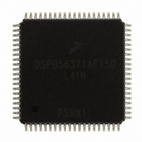
Manufacturer Part Number
DSPB56371AF150
Description
IC DSP 24BIT 150MHZ 80-LQFP
Manufacturer
Freescale Semiconductor
Series
Symphony™r
Type
Audio Processorr
Datasheet
1.DSPB56371AF180.pdf
(68 pages)
Specifications of DSPB56371AF150
Interface
Host Interface, I²C, SAI, SPI
Clock Rate
150MHz
Non-volatile Memory
ROM (384 kB)
On-chip Ram
264kB
Voltage - I/o
3.30V
Voltage - Core
1.25V
Operating Temperature
-40°C ~ 115°C
Mounting Type
Surface Mount
Package / Case
80-LQFP
Product
DSPs
Data Bus Width
24 bit
Processor Series
DSP563xx
Core
56000
Numeric And Arithmetic Format
Fixed-Point
Device Million Instructions Per Second
150 MIPs
Maximum Clock Frequency
150 MHz
Program Memory Size
192 KB
Data Ram Size
264 KB
Operating Supply Voltage
1.25 V, 3.3 V
Maximum Operating Temperature
+ 115 C
Mounting Style
SMD/SMT
Minimum Operating Temperature
- 40 C
Lead Free Status / RoHS Status
Lead free / RoHS Compliant
Available stocks
Company
Part Number
Manufacturer
Quantity
Price
Company:

Part Number:
DSPB56371AF150
Manufacturer:
Freescale Semiconductor
Quantity:
10 000
Part Number:
DSPB56371AF150
Manufacturer:
FREESCALE
Quantity:
20 000


Freescale Semiconductor
Signal Name
FSR_1
FST_1
PE1
PE4
Input, output, or
Input, output, or
Input or output
Input or output
disconnected
disconnected
Signal Type
Table 9. Enhanced Serial Audio Interface_1 Signals
State during
disconnected
disconnected
Reset
GPIO
GPIO
DSP56371 Data Sheet, Rev. 4.1
Frame Sync for Receiver_1—This is the receiver frame sync
input/output signal. In the asynchronous mode (SYN=0), the
FSR_1 pin operates as the frame sync input or output used by all
the enabled receivers. In the synchronous mode (SYN=1), it
operates as either the serial flag 1 pin (TEBE=0), or as the
transmitter external buffer enable control (TEBE=1, RFSD=1).
When this pin is configured as serial flag pin, its direction is
determined by the RFSD bit in the RCCR_1 register. When
configured as the output flag OF1, this pin will reflect the value of
the OF1 bit in the SAICR_1 register, and the data in the OF1 bit
will show up at the pin synchronized to the frame sync in normal
mode or the slot in network mode. When configured as the input
flag IF1, the data value at the pin will be stored in the IF1 bit in the
SAISR register, synchronized by the frame sync in normal mode
or the slot in network mode.
Port E1—When the ESAI_1 is configured as GPIO, this signal is
individually programmable as input, output, or internally
disconnected.
The default state after reset is GPIO disconnected.
Internal Pull down resistor.
This input is 5 V tolerant.
Frame Sync for Transmitter_1—This is the transmitter frame
sync input/output signal. For synchronous mode, this signal is the
frame sync for both transmitters and receivers. For asynchronous
mode, FST_1 is the frame sync for the transmitters only. The
direction is determined by the transmitter frame sync direction
(TFSD) bit in the ESAI_1 transmit clock control register
(TCCR_1).
Port E4—When the ESAI_1 is configured as GPIO, this signal is
individually programmable as input, output, or internally
disconnected.
The default state after reset is GPIO disconnected.
Internal Pull down resistor.
This input is 5 V tolerant.
Signal Description
Signal/Connection Descriptions
25
Related parts for DSPB56371AF150
Image
Part Number
Description
Manufacturer
Datasheet
Request
R

Part Number:
Description:
Manufacturer:
Freescale Semiconductor, Inc
Datasheet:
Part Number:
Description:
Manufacturer:
Freescale Semiconductor, Inc
Datasheet:
Part Number:
Description:
Manufacturer:
Freescale Semiconductor, Inc
Datasheet:
Part Number:
Description:
Manufacturer:
Freescale Semiconductor, Inc
Datasheet:
Part Number:
Description:
Manufacturer:
Freescale Semiconductor, Inc
Datasheet:
Part Number:
Description:
Manufacturer:
Freescale Semiconductor, Inc
Datasheet:
Part Number:
Description:
Manufacturer:
Freescale Semiconductor, Inc
Datasheet:
Part Number:
Description:
Manufacturer:
Freescale Semiconductor, Inc
Datasheet:
Part Number:
Description:
Manufacturer:
Freescale Semiconductor, Inc
Datasheet:
Part Number:
Description:
Manufacturer:
Freescale Semiconductor, Inc
Datasheet:
Part Number:
Description:
Manufacturer:
Freescale Semiconductor, Inc
Datasheet:
Part Number:
Description:
Manufacturer:
Freescale Semiconductor, Inc
Datasheet:
Part Number:
Description:
Manufacturer:
Freescale Semiconductor, Inc
Datasheet:
Part Number:
Description:
Manufacturer:
Freescale Semiconductor, Inc
Datasheet:
Part Number:
Description:
Manufacturer:
Freescale Semiconductor, Inc
Datasheet: