DSPB56371AF150 Freescale Semiconductor, DSPB56371AF150 Datasheet - Page 6
DSPB56371AF150
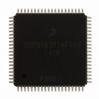
Manufacturer Part Number
DSPB56371AF150
Description
IC DSP 24BIT 150MHZ 80-LQFP
Manufacturer
Freescale Semiconductor
Series
Symphony™r
Type
Audio Processorr
Datasheet
1.DSPB56371AF180.pdf
(68 pages)
Specifications of DSPB56371AF150
Interface
Host Interface, I²C, SAI, SPI
Clock Rate
150MHz
Non-volatile Memory
ROM (384 kB)
On-chip Ram
264kB
Voltage - I/o
3.30V
Voltage - Core
1.25V
Operating Temperature
-40°C ~ 115°C
Mounting Type
Surface Mount
Package / Case
80-LQFP
Product
DSPs
Data Bus Width
24 bit
Processor Series
DSP563xx
Core
56000
Numeric And Arithmetic Format
Fixed-Point
Device Million Instructions Per Second
150 MIPs
Maximum Clock Frequency
150 MHz
Program Memory Size
192 KB
Data Ram Size
264 KB
Operating Supply Voltage
1.25 V, 3.3 V
Maximum Operating Temperature
+ 115 C
Mounting Style
SMD/SMT
Minimum Operating Temperature
- 40 C
Lead Free Status / RoHS Status
Lead free / RoHS Compliant
Available stocks
Company
Part Number
Manufacturer
Quantity
Price
Company:

Part Number:
DSPB56371AF150
Manufacturer:
Freescale Semiconductor
Quantity:
10 000
Part Number:
DSPB56371AF150
Manufacturer:
FREESCALE
Quantity:
20 000


DSP56371 Overview
2.4.2
The AGU performs the effective address calculations using integer arithmetic necessary to address data
operands in memory and contains the registers used to generate the addresses. It implements four types of
arithmetic: linear, modulo, multiple wrap-around modulo and reverse-carry. The AGU operates in parallel
with other chip resources to minimize address-generation overhead.
The AGU is divided into two halves, each with its own Address ALU. Each Address ALU has four sets of
register triplets, and each register triplet is composed of an address register, an offset register and a
modifier register. The two Address ALUs are identical. Each contains a 24-bit full adder (called an offset
adder).
A second full adder (called a modulo adder) adds the summed result of the first full adder to a modulo
value that is stored in its respective modifier register. A third full adder (called a reverse-carry adder) is
also provided.
The offset adder and the reverse-carry adder are in parallel and share common inputs. The only difference
between them is that the carry propagates in opposite directions. Test logic determines which of the three
summed results of the full adders is output.
Each Address ALU can update one address register from its respective address register file during one
instruction cycle. The contents of the associated modifier register specifies the type of arithmetic to be used
in the address register update calculation. The modifier value is decoded in the Address ALU.
2.4.3
The PCU performs instruction prefetch, instruction decoding, hardware DO loop control and exception
processing. The PCU implements a seven-stage pipeline and controls the different processing states of the
DSP56300 core. The PCU consists of the following three hardware blocks:
The PDC decodes the 24-bit instruction loaded into the instruction latch and generates all signals necessary
for pipeline control. The PAG contains all the hardware needed for program address generation, system
stack and loop control. The Program interrupt controller arbitrates among all interrupt requests (internal
interrupts, as well as the five external requests: IRQA, IRQB, IRQC, IRQD and NMI) and generates the
appropriate interrupt vector address.
PCU features include the following:
6
•
•
•
•
•
•
•
•
•
Program decode controller (PDC)
Program address generator (PAG)
Program interrupt controller
Position independent code support
Addressing modes optimized for DSP applications (including immediate offsets)
On-chip instruction cache controller
On-chip memory-expandable hardware stack
Nested hardware DO loops
Fast auto-return interrupts
Address Generation Unit (AGU)
Program Control Unit (PCU)
DSP56371 Data Sheet, Rev. 4.1
Freescale Semiconductor
Related parts for DSPB56371AF150
Image
Part Number
Description
Manufacturer
Datasheet
Request
R

Part Number:
Description:
Manufacturer:
Freescale Semiconductor, Inc
Datasheet:
Part Number:
Description:
Manufacturer:
Freescale Semiconductor, Inc
Datasheet:
Part Number:
Description:
Manufacturer:
Freescale Semiconductor, Inc
Datasheet:
Part Number:
Description:
Manufacturer:
Freescale Semiconductor, Inc
Datasheet:
Part Number:
Description:
Manufacturer:
Freescale Semiconductor, Inc
Datasheet:
Part Number:
Description:
Manufacturer:
Freescale Semiconductor, Inc
Datasheet:
Part Number:
Description:
Manufacturer:
Freescale Semiconductor, Inc
Datasheet:
Part Number:
Description:
Manufacturer:
Freescale Semiconductor, Inc
Datasheet:
Part Number:
Description:
Manufacturer:
Freescale Semiconductor, Inc
Datasheet:
Part Number:
Description:
Manufacturer:
Freescale Semiconductor, Inc
Datasheet:
Part Number:
Description:
Manufacturer:
Freescale Semiconductor, Inc
Datasheet:
Part Number:
Description:
Manufacturer:
Freescale Semiconductor, Inc
Datasheet:
Part Number:
Description:
Manufacturer:
Freescale Semiconductor, Inc
Datasheet:
Part Number:
Description:
Manufacturer:
Freescale Semiconductor, Inc
Datasheet:
Part Number:
Description:
Manufacturer:
Freescale Semiconductor, Inc
Datasheet: