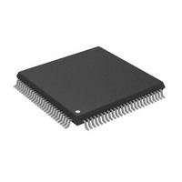
ADSP-2186KSTZ-133 Analog Devices Inc, ADSP-2186KSTZ-133 Datasheet - Page 27

ADSP-2186KSTZ-133
Manufacturer Part Number
ADSP-2186KSTZ-133
Description
IC DSP CONTROLLER 16BIT 100LQFP
Manufacturer
Analog Devices Inc
Series
ADSP-21xxr
Type
Fixed Pointr
Datasheet
1.ADSP-2186BSTZ-160.pdf
(36 pages)
Specifications of ADSP-2186KSTZ-133
Interface
Host Interface, Serial Port
Clock Rate
33.3MHz
Non-volatile Memory
External
On-chip Ram
40kB
Voltage - I/o
5.00V
Voltage - Core
5.00V
Operating Temperature
0°C ~ 70°C
Mounting Type
Surface Mount
Package / Case
100-LQFP
Device Core Size
16b
Format
Fixed Point
Clock Freq (max)
33.3MHz
Mips
33.3
Device Input Clock Speed
33.3MHz
Ram Size
40KB
Operating Supply Voltage (typ)
5V
Operating Supply Voltage (min)
4.5V
Operating Supply Voltage (max)
5.5V
Operating Temp Range
0C to 70C
Operating Temperature Classification
Commercial
Mounting
Surface Mount
Pin Count
100
Package Type
LQFP
Lead Free Status / RoHS Status
Lead free / RoHS Compliant
OUTPUT DRIVE CURRENTS
Figure 22 shows typical I-V characteristics for the output drivers
of the ADSP-2186. The curves represent the current drive
capability of the output drivers as a function of output voltage.
POWER DISSIPATION
To determine total power dissipation in a specific application,
the following equation should be applied for each output:
C = load capacitance, f = output switching frequency.
Example
In an application where external data memory is used and no
other outputs are active, power dissipation is calculated as follows:
Assumptions
• External data memory is accessed every cycle with 50% of the
• External data memory writes occur every other cycle with
• Each address and data pin has a 10 pF total load at the pin.
• The application operates at V
P
graph (Figure 23).
(C × V
Address
Data Output, WR 9
RD
CLKOUT, DMS 2
Total power dissipation for this example is PINT + 105 mW.
INT
address pins switching.
50% of the data pins switching.
= internal power dissipation from Power vs. Frequency
DD
–20
–40
–60
–80
60
40
20
Total Power Dissipation = P
2
0
0
× f) is calculated for each output:
V
OH
1
# of
Pins
7
1
× 10 pF × 5
× 10 pF × 5
× 10 pF × 5
× 10 pF × 5
SOURCE VOLTAGE – Volts
2
C × V
C
4.5V, +85 C
5.5V, –40 C
DD
DD
3
2
= 5.0 V and t
INT
× f
V
2
2
2
2
DD
V
V
V
V
+ (C × V
2
4.5V, +85 C
5.0V, +25 C
5.5V, –40 C
4
× 20 MHz = 35 mW
× 20 MHz = 45 mW
× 20 MHz =
× 40 MHz = 20 mW
5.0V, +25 C
f
DD
CK
5
2
= 30 ns.
× f)
V
OL
105 mW
6
5 mW
VALID FOR ALL TEMPERATURE GRADES.
1
2
3
4
POWER REFLECTS DEVICE OPERATING WITH NO OUTPUT LOADS.
TYPICAL POWER DISSIPATION AT 5.0V V
I
MEMORY. 50% OF THE INSTRUCTIONS ARE MULTIFUNCTION (TYPES 1, 4, 5, 12, 13, 14),
30% ARE TYPE 2 AND TYPE 6, AND 20% ARE IDLE INSTRUCTIONS.
IDLE REFERS TO ADSP-2186 STATE OF OPERATION DURING EXECUTION OF IDLE
INSTRUCTION. DEASSERTED PINS ARE DRIVEN TO EITHER V
DD
MEASUREMENT TAKEN WITH ALL INSTRUCTIONS EXECUTING FROM INTERNAL
100
500
400
300
200
100
80
60
40
20
80
60
40
20
0
0
0
34.7mW
32.8mW
330mW
250mW
180mW
62mW
82mW
62mW
45mW
2186 POWER, INTERNAL
33.33
33.33
33.33
POWER, IDLE n MODES
V
V
V
V
V
V
DD
POWER, IDLE
DD
DD
DD
DD
DD
= 5.5V
= 5.5V
= 5.0V
= 4.5V
= 4.5V
= 5.0V
1/tcyc – MHz
1/tcyc – MHz
1/tcyc – MHz
DD
AND T
70.5mW
36.6mW
34.3mW
1,2,4
A
= +25 C EXCEPT WHERE SPECIFIED.
40
40
40
1,2,3
ADSP-2186
2
385mW
300mW
225mW
91.5mW
70.5mW
52mW
IDLE
IDLE (16)
IDLE (128)
DD
OR GND.


