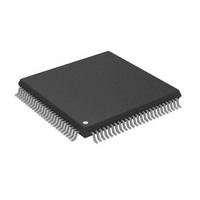
ADSP-2186KSTZ-133 Analog Devices Inc, ADSP-2186KSTZ-133 Datasheet - Page 8

ADSP-2186KSTZ-133
Manufacturer Part Number
ADSP-2186KSTZ-133
Description
IC DSP CONTROLLER 16BIT 100LQFP
Manufacturer
Analog Devices Inc
Series
ADSP-21xxr
Type
Fixed Pointr
Datasheet
1.ADSP-2186BSTZ-160.pdf
(36 pages)
Specifications of ADSP-2186KSTZ-133
Interface
Host Interface, Serial Port
Clock Rate
33.3MHz
Non-volatile Memory
External
On-chip Ram
40kB
Voltage - I/o
5.00V
Voltage - Core
5.00V
Operating Temperature
0°C ~ 70°C
Mounting Type
Surface Mount
Package / Case
100-LQFP
Device Core Size
16b
Format
Fixed Point
Clock Freq (max)
33.3MHz
Mips
33.3
Device Input Clock Speed
33.3MHz
Ram Size
40KB
Operating Supply Voltage (typ)
5V
Operating Supply Voltage (min)
4.5V
Operating Supply Voltage (max)
5.5V
Operating Temp Range
0C to 70C
Operating Temperature Classification
Commercial
Mounting
Surface Mount
Pin Count
100
Package Type
LQFP
Lead Free Status / RoHS Status
Lead free / RoHS Compliant
ADSP-2186
The master reset sets all internal stack pointers to the empty
stack condition, masks all interrupts and clears the MSTAT
register. When RESET is released, if there is no pending bus
request and the chip is configured for booting, the boot-loading
sequence is performed. The first instruction is fetched from
on-chip program memory location 0x0000 once boot loading
completes.
MEMORY ARCHITECTURE
The ADSP-2186 provides a variety of memory and peripheral
interface options. The key functional groups are Program Memory,
Data Memory, Byte Memory and I/O.
Program Memory (Full Memory Mode) is a 24-bit-wide space
for storing both instruction opcodes and data. The ADSP-2186
has 8K words of Program Memory RAM on chip, and the capabil-
ity of accessing up to two 8K external memory overlay spaces using
the external data bus. Both an instruction opcode and a data value
can be read from on-chip program memory in a single cycle.
Data Memory (Full Memory Mode) is a 16-bit-wide space
used for the storage of data variables and for memory-mapped
control registers. The ADSP-2186 has 8K words on Data
Memory RAM on chip, consisting of 8160 user-accessible
locations and 32 memory-mapped registers. Support also exists
for up to two 8K external memory overlay spaces through the
external data bus.
Byte Memory (Full Memory Mode) provides access to an
8-bit wide memory space through the Byte DMA (BDMA) port.
The Byte Memory interface provides access to 4 MBytes of
memory by utilizing eight data lines as additional address lines.
This gives the BDMA Port an effective 22-bit address range. On
power-up, the DSP can automatically load bootstrap code from
byte memory.
I/O Space (Full Memory Mode) allows access to 2048 loca-
tions of 16-bit-wide data. It is intended to be used to communi-
cate with parallel peripheral devices such as data converters and
external registers or latches.
Program Memory
The ADSP-2186 contains an 8K × 24 on-chip program RAM.
The on-chip program memory is designed to allow up to two
accesses each cycle so that all operations can complete in a
single cycle. In addition, the ADSP-2186 allows the use of 8K
external memory overlays.
The program memory space organization is controlled by the
Mode B pin and the PMOVLAY register. Normally, the ADSP-
2186 is configured with Mode B = 0 and program memory
organized as shown in Figure 4.
PROGRAM MEMORY
(PMOVLAY = 1 or 2,
EXTERNAL 8K
8K INTERNAL
MODE B = 0)
ADDRESS
0x3FFF
0x2000
0x1FFF
0x0000
There are 8K words of memory accessible internally when the
PMOVLAY register is set to 0. When PMOVLAY is set to some-
thing other than 0, external accesses occur at addresses 0x2000
through 0x3FFF. The external address is generated as shown in
Table II.
PMOVLAY Memory
0
1
2
NOTE: Addresses 0x2000 through 0x3FFF should not be accessed when
PMOVLAY = 0.
This organization provides for two external 8K overlay segments
using only the normal 14 address bits, which allows for simple
program overlays using one of the two external segments in
place of the on-chip memory. Care must be taken in using this
overlay space in that the processor core (i.e., the sequencer)
does not take into account the PMOVLAY register value. For
example, if a loop operation is occurring on one of the external
overlays and the program changes to another external overlay or
internal memory, an incorrect loop operation could occur. In
addition, care must be taken in interrupt service routines as the
overlay registers are not automatically saved and restored on the
processor mode stack.
When Mode B = 1, booting is disabled and overlay memory is
disabled (PMOVLAY must be 0). Figure 5 shows the memory
map in this configuration.
Data Memory
The ADSP-2186 has 8160 16-bit words of internal data memory.
In addition, the ADSP-2186 allows the use of 8K external memory
overlays. Figure 6 shows the organization of the data memory.
Reserved
External
Overlay 1
External
Overlay 2
Table II. PMOVLAY Addressing
PROGRAM MEMORY
MAPPED REGISTERS
(DMOVLAY = 1, 2)
DATA MEMORY
8K EXTERNAL
RESERVED
EXTERNAL 8K
32 MEMORY–
8160 WORDS
INTERNAL
A13
Not Applicable Not Applicable
0
1
ADDRESS
ADDRESS
0x3FFF
0x2000
0x1FFF
0x0000
0x3FFF
0x3FEO
0x3FDF
0x2000
0x1FFF
0x0000
A12:0
13 LSBs of Address
Between 0x2000
and 0x3FFF
13 LSBs of Address
Between 0x2000
and 0x3FFF


