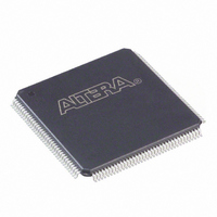
EP2C8T144C7N Altera, EP2C8T144C7N Datasheet - Page 43

EP2C8T144C7N
Manufacturer Part Number
EP2C8T144C7N
Description
IC CYCLONE II FPGA 8K 144-TQFP
Manufacturer
Altera
Series
Cyclone® IIr
Datasheet
1.EP2C5T144C8N.pdf
(168 pages)
Specifications of EP2C8T144C7N
Number Of Logic Elements/cells
8256
Number Of Labs/clbs
516
Total Ram Bits
165888
Number Of I /o
85
Voltage - Supply
1.15 V ~ 1.25 V
Mounting Type
Surface Mount
Operating Temperature
0°C ~ 85°C
Package / Case
144-TQFP, 144-VQFP
Lead Free Status / RoHS Status
Lead free / RoHS Compliant
Number Of Gates
-
Other names
544-1667
Available stocks
Company
Part Number
Manufacturer
Quantity
Price
Company:
Part Number:
EP2C8T144C7N
Manufacturer:
Altera
Quantity:
135
Company:
Part Number:
EP2C8T144C7N
Manufacturer:
ATLERA
Quantity:
10
Altera Corporation
February 2007
Clock Modes
Table 2–8
memory.
Table 2–9
when configured in the different memory modes.
M4K Routing Interface
The R4, C4, and direct link interconnects from adjacent LABs drive the
M4K block local interconnect. The M4K blocks can communicate with
LABs on either the left or right side through these row resources or with
LAB columns on either the right or left with the column resources. Up to
16 direct link input connections to the M4K block are possible from the
left adjacent LAB and another 16 possible from the right adjacent LAB.
M4K block outputs can also connect to left and right LABs through each
16 direct link interconnects.
array interface.
Independent
Input/output
Read/write
Single
Independent
Input/output
Read/write
Single clock
Table 2–8. M4K Clock Modes
Clock Mode
Table 2–9. Cyclone II M4K Memory Clock Modes
Clocking Modes
summarizes the different clock modes supported by the M4K
shows which clock modes are supported by all M4K blocks
In this mode, a separate clock is available for each port (ports A
and B). Clock A controls all registers on the port A side, while
clock B controls all registers on the port B side.
On each of the two ports, A or B, one clock controls all registers
for inputs into the memory block: data input, wren, and address.
The other clock controls the block’s data output registers.
Up to two clocks are available in this mode. The write clock
controls the block’s data inputs, wraddress, and wren. The
read clock controls the data output, rdaddress, and rden.
control all registers of the memory block. Asynchronous clear
signals for the registers are not supported.
In this mode, a single clock, together with clock enable, is used to
True Dual-Port
Mode
v
v
v
Figure 2–17
Cyclone II Device Handbook, Volume 1
Simple Dual-Port
Description
shows the M4K block to logic
Mode
v
v
v
Cyclone II Architecture
Single-Port Mode
v
v
2–31


